Menu

Blog

Archive for the ‘materials’ category: Page 261

Feb 27, 2017

Chiral superconductivity experimentally demonstrated for the first time

Posted by in categories: materials, nanotechnology

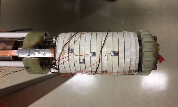
(Phys.org)—Scientists have found that a superconducting current flows in only one direction through a chiral nanotube, marking the first observation of the effects of chirality on superconductivity. Until now, superconductivity has only been demonstrated in achiral materials, in which the current flows in both directions equally.

The team of researchers, F. Qin et al., from Japan, the US, and Israel, have published a paper on the first observation of chiral in a recent issue of Nature Communications.

Chiral superconductivity combines two typically unrelated concepts in a single material: Chiral materials have mirror images that are not identical, similar to how left and right hands are not identical because they cannot be superimposed one on top of the other. And superconducting materials can conduct an electric current with zero resistance at very low temperatures.

Continue reading “Chiral superconductivity experimentally demonstrated for the first time” »

Feb 27, 2017

Universal Everything’s Futuristic Prototypes Build on Humanity’s Relationship With Technology

Posted by in categories: futurism, materials

‘screens of the future’ is a digital series of protuct prototypes based on the emerging technologies of flexible display and shape-shifting materials.

Read more

Feb 26, 2017

New metamaterial is proved to be the world’s first to achieve the performance predicted by theoretical bounds

Posted by in categories: materials, transportation

In 2015 UC Santa Barbara mechanical engineer and materials scientist Jonathan Berger developed an idea that could change the way people think about high-performance structural materials. Two years later, his concept is paying research dividends.

In a letter published in the journal Nature, Berger, with UCSB materials and mechanical engineering professor Robert McMeeking and materials scientist Haydn N. G. Wadley from the University of Virginia, prove that the three-dimensional pyramid-and-cross cell geometry Berger conceived is the first of its kind to achieve the performance predicted by theoretical bounds. Its lightness, strength and versatility, according to Berger, lends itself well to a variety of applications, from buildings to vehicles to packaging and transport.

Called Isomax, the beauty of this solid foam—in this case loosely defined as a combination of a stiff substance and air pockets—lay in the geometry within. Instead of the typical assemblage of bubbles or a honeycomb arrangement, the ordered cells were set apart by walls forming the shapes of pyramids with three sides and a base, and octahedra, reinforced inside with a “cross” of intersecting diagonal walls.

Continue reading “New metamaterial is proved to be the world’s first to achieve the performance predicted by theoretical bounds” »

Feb 23, 2017

Nano Thread Enables Scientists to Extend Length of Brain Implant Efficacy

Posted by in categories: materials, neuroscience

There is way more coming in BMI.


Researcher Dr. Luan and his interdisciplinary team from the University of Texas at Austin have developed an ultra flexible nanoelectronic thread (NET) that has the potential to offer a new type of the long-term neural implants. Neural probes are used to directly measure or even stimulate electrical activity in specific regions of the brain. However, despite the many advances in the field, issues with biocompatibility have limited the prospects and usefulness of the technology. Conventional probes induce scarring around the implant over time, which in turn increasingly impairs the devices’ ability to measure electrical impulses. This scarring is a result of conventional probes’ width, material, and lack of flexibility.

Due to the micrometer dimensions of the NET and its insulation, the implant doesn’t trigger the development of scar tissue and continues working for months at a time. Publishing in the journal Science Advances, the researchers describe the NET from 7 nm nanoprobes layered together and two to three layers of insulation. The layers together total to about 1 µm in thickness, which grants the probe flexibility that is almost 1000 times greater than conventional probes. This flexibility allows the device to remain in place without hindering the movement of or displacing surrounding tissue.

Continue reading “Nano Thread Enables Scientists to Extend Length of Brain Implant Efficacy” »

Feb 23, 2017

Nano-size revolution is getting bigger

Posted by in categories: materials, nanotechnology

And, we just started. Just wait — in the next 6 to 8 months; I will some amazing news to share on QBS and BMI. smile


An explosion of nanotechnology research and development is occurring as newly identified forms of carbon, including graphene, carbon nanotubes and nano-diamonds, pave the way for new products and industries.

This article is sponsored by Flinders University.

Continue reading “Nano-size revolution is getting bigger” »

Feb 23, 2017

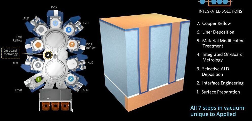
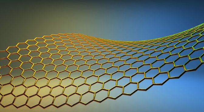
Graphene Could Buttress Next-Gen Computer Chip Wiring

Posted by in categories: computing, materials

Nice.


Current can literally blow copper interconnects away, but graphene could keep them intact.

Read more

Feb 23, 2017

Synopsis: Revealing a Hidden Spin Polarization

Posted by in category: materials

Photoemission spectroscopy has detected two different populations of spin-polarized electrons that are “hidden” within a layered, graphene-like material.

The layers inside certain materials can carry spin-polarized electrons, but this polarization is hidden to measurements that aren’t sufficiently localized. A new study using photoemission spectroscopy has detected the hidden spin polarization in a graphene-like material called molybdenum disulfide (MoS22). Unique to this work is the ability to target specific populations of spin-polarized electrons with circularly polarized light.

Read more

Feb 21, 2017

Shell-Dependent Photoluminescence Studies Provide Mechanistic Insights into the Off-Grey-On Transitions of Blinking Quantum Dots

Posted by in categories: materials, quantum physics

The majority of quantum dot (QD) blinking studies have used a model of switching between two distinct fluorescence intensity levels, “on” and “off”. However, a distinct intermediate intensity level has been identified in some recent reports – a so-called “grey” or “dim” state, which has brought this binary model into question. While this grey state has been proposed to result from the formation of a trion, it is still unclear under which conditions it is present in a QD. By performing shell-dependent blinking studies on CdSe QDs, we report that the populations of the grey state and the on state are strongly dependent on both the shell material and its thickness. We found that adding a ZnS shell did not result in a significant population of the grey state. Using ZnSe as the shell material resulted in a slightly higher population of the grey state, although it was still poorly resolved. However, adding a CdS shell resulted in the population of a grey state, which depended strongly on its thickness up to 5 ML. Interestingly, while the frequency of transitions to and from the grey state showed a very strong dependence on CdS shell thickness, the brightness of and the dwell time in the grey state did not. Moreover, we found that the grey state acts as an on-pathway intermediate state between on and off states, with the thickness of the shell determining the transition probability between them. We also identified two types of blinking behavior in QDs, one that showed long-lived but lower intensity on states and another that showed short-lived but brighter on states that also depended on the shell thickness. Intensity-resolved single QD fluorescence lifetime analysis was used to identify the relationship between the various exciton decay pathways and the resulting intensity levels. We used this data to propose a model in which multiple on, grey and off states exist whose equilibrium populations vary with time that give rise to the various intensity levels of single QDs, and which depends on shell composition and thickness.

View: PDF | PDF w/ Links.

Read more

Feb 18, 2017

Graphene-based processors could make your computer fast AF

Posted by in categories: computing, materials

Read more

Feb 14, 2017

Controlling Friction Levels through On/Off Application of Laser Light

Posted by in category: materials

A NIMS research group led by Masahiro Goto, Distinguished Chief Researcher, Center for Green Research on Energy and Environmental Materials, and Michiko Sasaki, postdoctoral researcher, Center for Materials Research by Information Integration (currently a postdoctoral fellow at the University of Tokyo) discovered that the amount of friction force between organic molecules and a sapphire substrate in a vacuum can be changed repeatedly by starting and stopping laser light irradiation. This discovery could potentially lead to the development of technology enabling the movement of micromachines and other small driving parts to be controlled.

The performance of micromachines—used as moving components in small devices such as acceleration sensors and gyroscopes—is greatly affected by adhesion force (the attractive force between two or more materials that stick to each other). Adhesion force in a micromachine increases the friction force. Since increased friction force seriously impedes the movement of moving components, it is necessary to maintain a low level of adhesion force. In addition, if the level of friction force can be controlled, it may be feasible to control the movement of micromachines, leading to expansion of their use and enhancement of their functions. A great deal of attention was previously drawn to techniques enabling silicon-based materials, a major micromachine material, to be coated with diamond-like carbon, self-assembled monolayers, or fluorine-containing organic films in order to reduce friction force and thereby improve the movement of micromachines.

Read more