By remotely accessing an IBM quantum computer, a research scientist at Lawrence Berkeley National Laboratory has successfully simulated a key process in particle physics: hadronization. Although based on a simplified model of quantum mechanics, the project lays the groundwork for how physicists can leverage the power of quantum computers to make large scientific calculations beyond the capabilities of classical supercomputers. The research is published in the journal Physical Review D.
Hadronization occurs when two or more quarks—the subatomic building blocks of matter—bind together through the strong nuclear force to form composite particles called hadrons. The most familiar examples of hadrons are protons and neutrons, which form the nuclei of atoms. So, having a better understanding of the hadronization process means having a better understanding of the structure of matter, and—in turn—the universe.
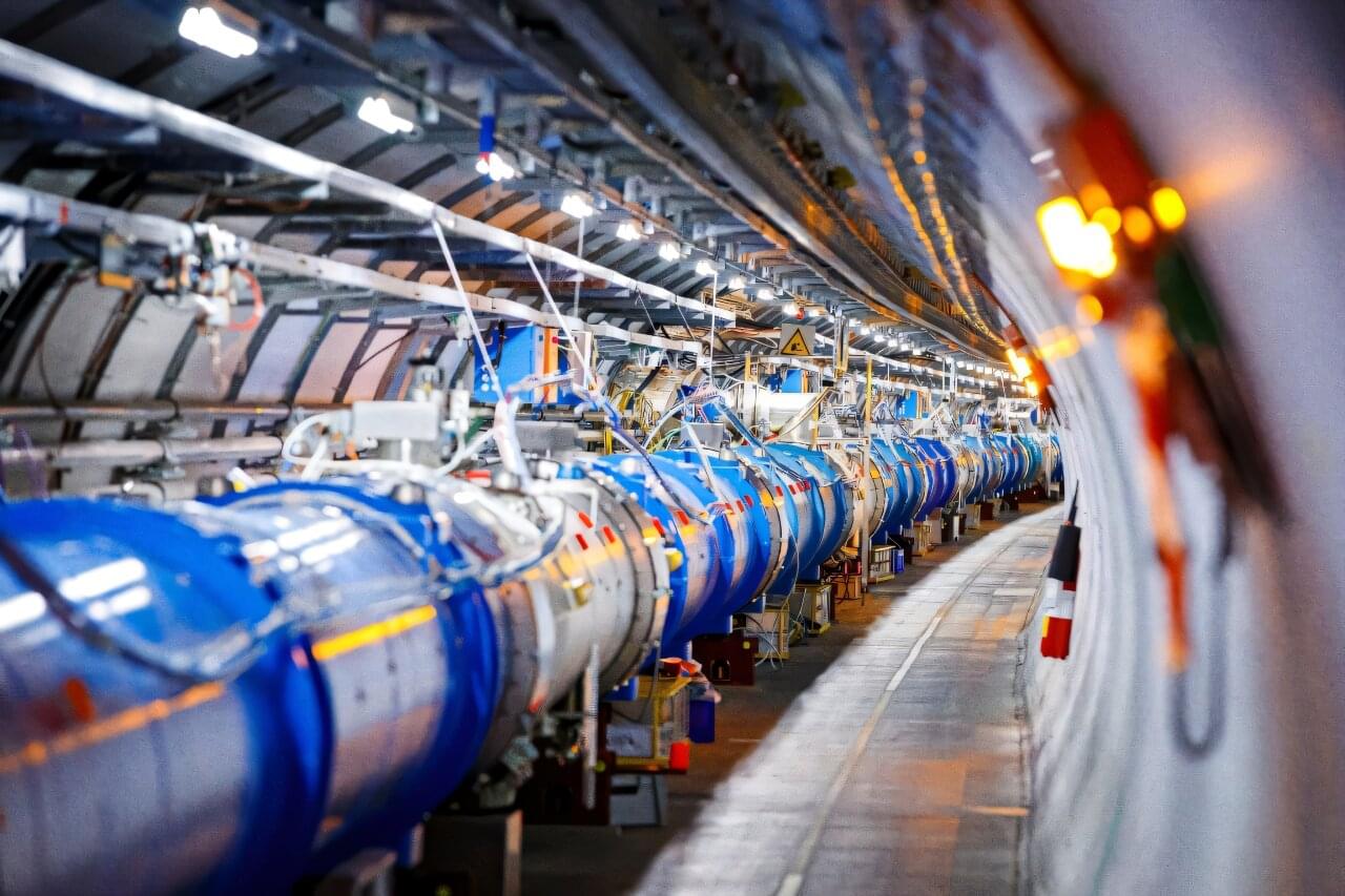
Physical experiments have not been able to reveal every step of the process, however. Researchers at the Large Hadron Collider (LHC) at CERN accelerate protons to near light speeds, guide them into collisions and study the resulting debris of quarks and antiquarks. But these particles can only be indirectly measured before they immediately undergo hadronization—hence the need for computer simulations to fill in the gaps of these scientific observations.