Toggle light / dark theme

Lab-grown retinal cells show promise for new eye therapies

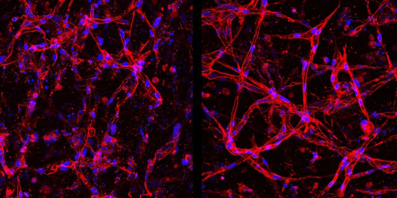
Biomedical engineers at Duke University have used induced pluripotent stem cells (iPSCs) to grow specialized blood vessel cells critical to retinal health for the first time. When injected into mouse models of retinal disease, these “retinal endothelial cells” integrated into the damaged tissue to regenerate blood vessels and restore retinal function. Researchers also demonstrated the cells’ ability to form functional retinal vascular tissue in a lab-grown environment, providing a pathway to model and research various eye diseases.

The results, published in the journal Nature Biomedical Engineering, point toward the potential of using these retinal cells and models to develop new methods for treating vision loss and researching eye disorders.

“Retinal vascular diseases affect millions of people in the US, but our understanding remains limited, hindering our ability to discover and develop new therapeutics,” said Sharon Gerecht, the Paul M. Gross Distinguished Professor and chair of biomedical engineering at Duke. “Using human stem cells, we generated the cells found in retinal blood vessels, paving the way for new therapeutic approaches.”

Wireless biodegradable sensor could help injured knees heal without dangerous overloading

A biodegradable pressure sensor could help people with knee injuries exercise and heal faster, University of Connecticut researchers report in Science Advances. The knee can take a great deal of abuse, thanks to the cartilage that cushions it. But if it’s not moved and exercised enough, the knee stiffens and has poor blood flow. The cartilage can degrade or tear, worsening any injury already there. So people with injured knees have to move in order to heal. The challenge is knowing how much exercise or movement is too much.

To answer that question, UConn College of Engineering professor Thanh Nguyen, along with Ph.D. student Jinyoung Park and other colleagues, developed a pressure sensor that can be placed inside the knee joint and then degrade harmlessly in the body when no longer needed.

“Overloading destroys the cartilage. But if you don’t move and exercise, if you don’t run, walk, jump, you have a very stiff joint with little blood flowing to it,” says Nguyen, a professor in the Department of Biomedical Engineering, which is a joint effort by the College of Engineering, School of Medicine and School of Dental Medicine. “My lab developed a sensor that can monitor the force in real time.”

Disorder creates direction-dependent optics in compound semiconductors

An international research team has demonstrated that the intrinsic disorder of the compound semiconductor CuInSnS₄ can be exploited to influence its optical properties. While the atomic vibrations also sense the local disorder, their response is averaged over many different local environments and therefore appears isotropic, as expected for a cubic crystal.

In contrast, the optical excitations, known as excitons, are much more sensitive to the local arrangement of atoms. Surprisingly, they show a direction-dependent optical response even though the average crystal structure is cubic. These findings shed new light on the relationship between disorder and material properties, opening new options for targeted “disorder engineering” in optoelectronic and photocatalytic devices.

Crystals are typically characterized by a periodic arrangement of atoms, in which each element occupies well-defined crystallographic sites throughout the structure. In compound semiconductors such as CuInSnS₄, a member of the adamantine chalcogenide family, the cations are ideally distributed over specific positions in the crystal structure.

Nanopattern method unlocks precise control of disorder for wave-guiding devices

A research team has developed a methodology to precisely design and control the “degree of disorder” in nanopattern arrays using metal-infiltrated block copolymer (BCP) thin films. The work was led by Professor So Youn Kim of the Seoul National University College of Engineering Department of Chemical and Biological Engineering, in collaboration with Professor Su-Mi Hur’s team at DGIST and Professor S. Joon Kwon’s team at Sungkyunkwan University. The paper is published in the journal Nature Communications. The study was selected as an Editors’ Highlight in materials science and chemistry.

This disordered nanopattern fabrication technology is regarded as an innovative approach that enables precise control of nanoscale disorder structures—previously difficult to regulate—thereby opening new possibilities in the design of nano-optical and nanoelectronic devices.

In ordered structures, waves propagate over long distances, whereas in disordered structures, repeated scattering can lead to localization, where waves remain confined within a specific region. Such disordered structures exhibit unique functionalities that can induce localization phenomena for various types of waves, including light, sound and heat.

Defect detection automated in diamond, other advanced semiconductors

Materials scientists at Rice University have developed a new workflow methodology for measuring microscopic defects in diamond and other advanced semiconductor materials. By making it easier to spot flaws that can undermine performance, the approach could accelerate the development of more reliable electronic and quantum devices.

The research team developed a custom Python-based software tool to rapidly analyze data from high-resolution X-ray diffraction, a technique that uses X-rays to probe a material’s internal crystal structure. The software analyzes the resulting diffraction patterns, picks up on dislocations and irregularities in the atomic lattice, and calculates their density in a given material.

“Dislocations can disrupt how charge and heat move through the material, which impacts how efficient and reliable a device is and how easy it is to manufacture at scale,” said Xiang Zhang, assistant research professor of materials science and nanoengineering at Rice and a corresponding author on the study published in Advanced Materials.

Artificial ‘leaf’ powers wireless biomedical device

Plants convert light into energy efficiently through photosynthesis—an ability that scientists and engineers still struggle to match with electronic devices. Recently, researchers have looked beyond traditional semiconductor materials to create devices using a promising class of materials called nanoplasmonics. These tiny metal structures can absorb and concentrate optical energy and generate energetic charge carriers.

In a new study, researchers from the University of Chicago Pritzker School of Molecular Engineering (UChicago PME) and Department of Chemistry developed a nanoplasmonic “leaf,” a wireless bioelectronic device they used to stimulate nerves and pace heartbeats in an animal model.

The team also showed that their material could be used as a computer-like sensing platform, where users can interact with the screen using invisible light—a potentially secure way to transmit information.

VR combined with nerve stimulation improves arm and hand function following a stroke

Researchers at the Medical University of Vienna and ETH Zurich have developed a rehabilitation platform for people suffering from the long-term effects of a stroke that combines virtual reality with targeted sensory nerve stimulation. In a randomized feasibility clinical study with stroke patients, recently published in Nature Medicine, the new technology contributed to improvements in arm and hand function, as well as in tactile and body awareness. These results open up the prospect of personalized and more accessible rehabilitation that can support patients’ recovery beyond the limits of conventional therapy.

Stroke is one of the leading causes of long-term disability worldwide. Even after intensive early physiotherapy, many stroke survivors continue to live with reduced arm and hand function, impaired sensation, and altered body awareness long after the initial event. While conventional rehabilitation can improve motor functions, it often focuses primarily on movement training; sensory deficits and body awareness are frequently given insufficient attention. There is therefore a need for more comprehensive rehabilitation strategies.

To address this need, a research team led by Stanisa Raspopovic (Center for Medical Physics and Biomedical Engineering, MedUni Vienna) has developed “MultiSensy,” a rehabilitation platform for patients with arm and hand impairments following a stroke that combines immersive virtual reality with transcutaneous electrical nerve stimulation. The system turns rehabilitation exercises into interactive virtual tasks designed to train specific arm and hand functions, including reaching, grasping, pinching and forearm rotation.

Modular coatings customize hydrogel implants to boost adhesion and limit fibrosis

Researchers led by Jiawei Yang, Worcester Polytechnic Institute (WPI) Assistant Professor in the Department of Mechanical and Materials Engineering, have designed a modular system that could potentially improve hydrogel implants in the body by customizing the materials for stiffness and functionality.

The system, described in the journal Science Advances, uses coatings to treat the surface of hydrogels, which are flexible, water-loaded polymers. The researchers reported that by customizing different types of hydrogels with unique coatings, they were able to create two distinct hydrogel implants that maintained adhesion in living tissue and resisted an immune system response.

“It is difficult for a material with a single chemical composition to play two distinct roles in an implant,” Yang said. “We addressed that by developing a way to customize hydrogel implants with two sets of chemical compositions that can be tailored to address specific needs and achieve better results.”

NASA just rolled a 3,100-ton machine 4 miles to the launch pad at less than 1 mph, the heaviest self-powered vehicle on Earth, carrying a Moon rocket that weighs less than the machine hauling it

When NASA sent four astronauts toward the Moon this spring, the cameras did what cameras always do at a launch. They pointed at the rocket. Artemis II was the first crew to fly around the Moon in more than 50 years, a 322-foot stack throwing fire over the Florida coast on April 1, and it earned every second of airtime it got.

But the rocket didn’t get itself to the launch pad. The machine that did is older than all four astronauts who flew the mission, weighs more than the rocket it carried, and moves so slowly you could lap it on foot without breaking a sweat. It is NASA’s Crawler-Transporter 2, and Guinness World Records lists it as the heaviest self-powered vehicle on the planet. While everyone watched the thing going up, the real engineering marvel spent the better part of a day going sideways at less than a mile an hour.

Start with the number that got it into the record books. Crawler-Transporter 2 weighs 6.65 million pounds, or about 3,106 metric tons. Guinness World Records made it official back in 2023 at a ceremony at Kennedy Space Center, handing NASA a certificate for the heaviest self-powered vehicle ever built. For scale, that is roughly the weight of 1,000 pickup trucks stacked on top of each other.

Copper thin films reveal ballistic electron transport that could reshape future chip wiring

A joint research team has experimentally observed ballistic transport in single-crystalline copper thin films, demonstrating that ballistic transport is achievable in an industry-standard metal at interconnect-relevant dimensions. The study, titled “Ballistic transport in nanodevices based on single-crystalline Cu thin films,” was published in Nature Communications.

Ballistic transport refers to a phenomenon in which electrons travel along straight trajectories without scattering. Until now, this behavior has mainly been observed in special quantum materials such as graphene or semiconductor nanostructures. In copper, where electron scattering is pronounced, realizing ballistic transport has been considered practically impossible.

In this study, the team led by Professor Gil-Ho Lee of the Department of Physics at POSTECH, Professor Emeritus Se-Young Jeong of the School of Transdisciplinary Engineering at Pusan National University and Professor Seong-Gon Kim of the Department of Physics and Astronomy at Mississippi State University, experimentally demonstrated that ballistic transport can occur in structures with a thickness of 80 nm and a linewidth of 150 nm, dimensions comparable to those used in semiconductor interconnects.

/* */