Researchers develope a 3D printing method for elastomer-based filaments that bend, twist, expand, or contract when heated or cooled.

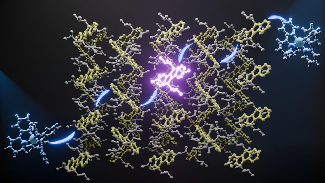
Two cups of warm water don’t make one cup of boiling water. But in the quantum world, multiple low-energy photons can combine to produce a single, higher-energy photon.
A research team at Kyushu University has developed a solid-state molecular material that “upgrades” visible light into ultraviolet (UV) light under ordinary outdoor sunlight, achieving a conversion efficiency of 1.9%. The study is published in Nature Communications.
Harsh UV light is something most people try to avoid in summer, yet it is indispensable in fields ranging from air purification and resin curing in 3D printing to gel hardening in dental fillings and nail art. Despite its importance, UV accounts for only about 6% of the sunlight reaching Earth’s surface, with only a fraction of that being practically usable.
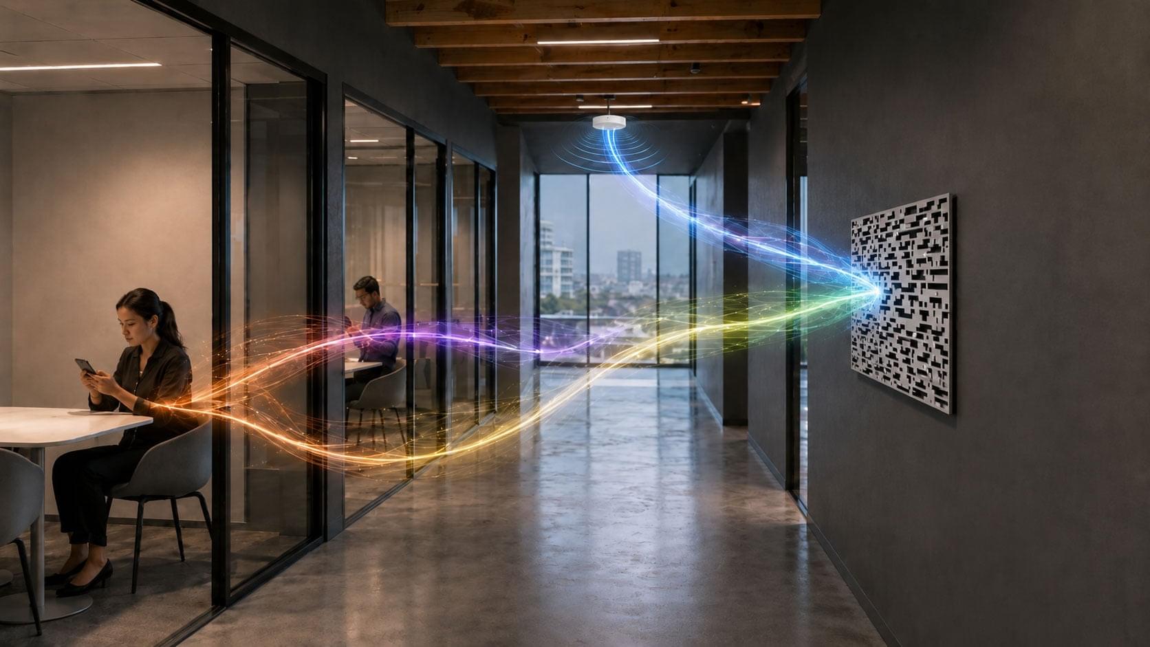

A passive 3D-printed panel could redirect wireless signals around corners without electronics or power. The metacrystal design can handle multiple incoming waves and different frequency bands, offering a lower-cost option for hard-to-reach indoor spaces.
Basements, tunnels, large buildings—a weak Wi-Fi or mobile signal in these hard-to-reach places is frustrating. The usual solution is to add more electronics like routers, repeaters and base stations. Yet, as we move towards a 6G mobile network, this kind of complex infrastructure can be unsustainable and prohibitively expensive. Higher-frequency channels of 6G communications aim to provide vastly more data bandwidth than the current 5G, but those channels are more easily blocked by walls, people and other obstacles.
To tackle this, researchers at Aalto University have developed a new solution in the form of metacrystals: passive, 3D-printed smart panels that can shape wireless signals without electronics, a power supply or active tuning. The paper, “Metacrystals: Inversely-designed 3D-printed intelligent panels for 6G communications” is published in Nature Communications.
“When a room is too dark, you can bring in more lamps—or use simple mirrors to guide the already available light. This is what these metacrystals do, but with radio waves,” explains doctoral researcher Mahdi Asgari. “Unlike previously proposed single-layer intelligent surfaces, these volumetric metacrystals can be designed to control multiple incoming signals or frequency bands independently—a key requirement for realistic wireless communication.”
Year 2024
Caption :
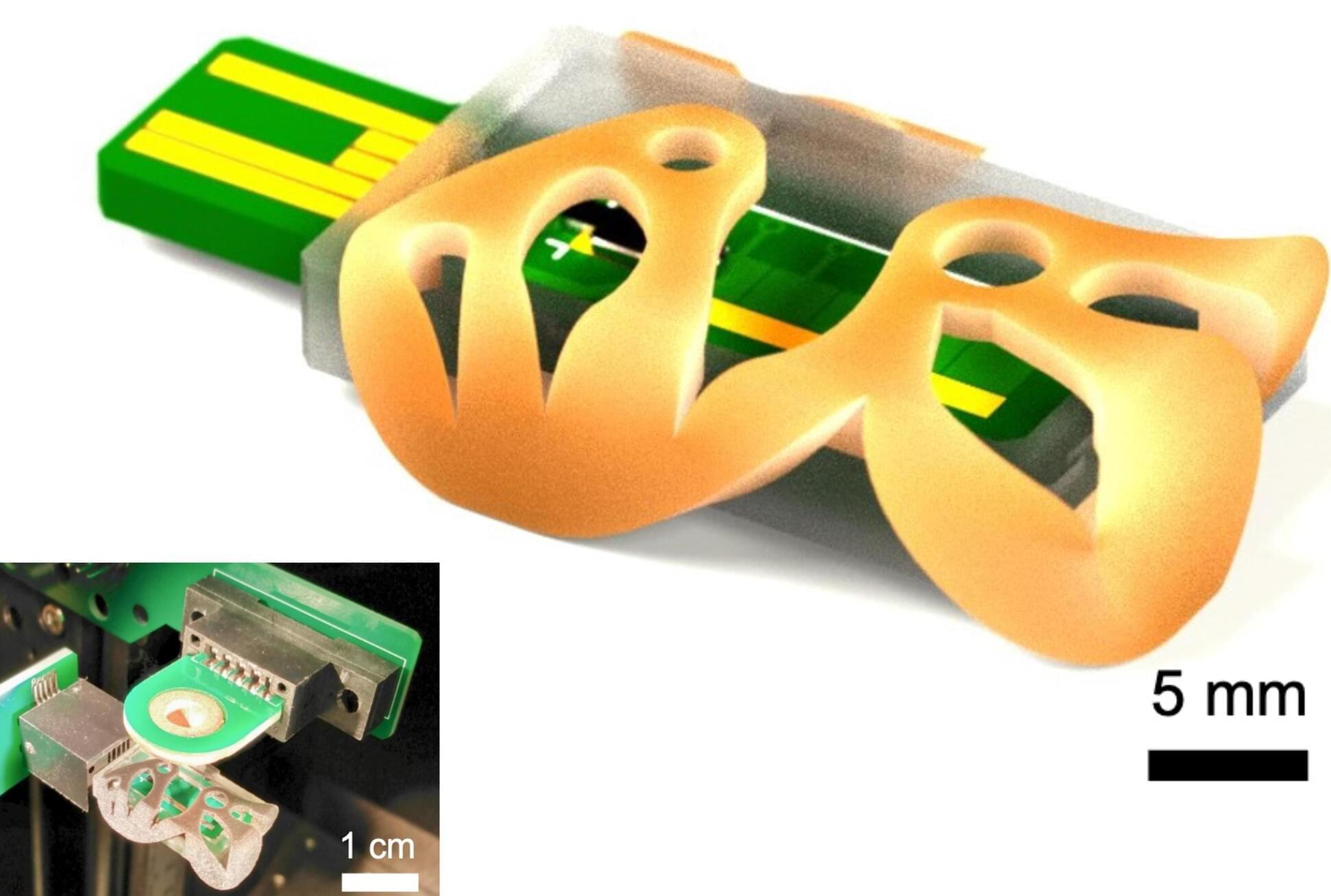
MIT researchers have 3D printed a miniature ionizer, which is a key component of a mass spectrometer. The new miniature ionizer could someday enable an affordable, in-home mass spectrometer for health monitoring. Pictured are parts of the new device, including a green printed circuit board (PCB) with orange casing on top. Under the casing is a black rectangle where the electrospray emitter is located.
Hi all, you should check out this human enhancement game created by Anton Kulaga and his team! You’ll learn about various genetic factors with potential for increasing human capabilities. The content is all rooted in scientific literature! Once you design a character, you can also get a 3D printed shape sent to you which is influenced by your choices.
Build your post-human character from real genes — tardigrade radiation shields, naked-mole-rat cancer resistance, Greenland shark longevity — backed by scientific evidence tiers and real citations. Spend enhancement credits and 3D-print the result.