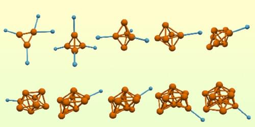
A technique combining spectroscopy and computational simulations allows the geometry and spin magnetic moment of iron nanoclusters to be determined more precisely.
“Advances in quantum research and development have shifted the risk horizon,” Mark Russinovich, chief technology officer of Microsoft Azure, said. “We believe cryptographically relevant quantum computers could arrive sooner than previously expected – and the work required to prepare is significant, so organizations need to start now.”
To that end, the Windows maker is speeding up the Microsoft Quantum Safe Program (QSP) timeline with the goal of transitioning critical products and services to post-quantum cryptography (PQC) by 2029. The company is also planning to incorporate PQC requirements into its Secure Future Initiative (SFI).
Some key focus areas include upgrading network cryptography by adopting TLS 1.3, building crypto-agility for stored data to facilitate the ability to change cryptography without having to redesign the underlying systems, and transitioning to PQC algorithms to secure trust chains, such as code signing, certificate issuance, key protection, and update pipelines.

The issues have been addressed in ColdFusion 2023 Update 21 and ColdFusion 2025 Update 10. Security researchers Anirudh Anand, Matan Sandori, and 2Bsecure have been credited with discovering and reporting CVE-2026–48283, CVE-2026–48313, and CVE-2026–48307.
Separately, Adobe has also shipped fixes to close out a critical flaw in Adobe Campaign Classic impacting versions ACC v7: 7.4.3 build 9,396 and earlier for Windows and Linux that could result in arbitrary code execution.
The vulnerability, tracked as CVE-2026–48286 (CVSS score: 10.0), is a case of incorrect authorization that could enable an attacker to execute arbitrary code on affected systems. It has been patched in version ACC v7: 7.4.3 build 9397.
Simple rules. Infinite complexity. Physicist Stephen Wolfram has spent forty years working out the connection. Here’s the short version.
❍ Subscribe to The Well on YouTube: https://bit.ly/welcometothewell.
❍ Up next: Why the answers to big questions are fundamentally unknowable | L.A. Paul • Why the answers to big decisions are funda…
Physicist Stephen Wolfram spent decades running computer experiments on simple rules — not looking for anything grand, just seeing what happened. What he found turned into a model of how the universe works, an explanation for why evolution never gets stuck, and a mathematical argument for why your life can’t be shortcut or predicted by anyone.
Read the full video transcript: https://bigthink.com/videos/the-unive…
❍ About The Well ❍
Do we inhabit a multiverse? Do we have free will? What is love? Is evolution directional? There are no simple answers to life’s biggest questions, and that’s why they’re the questions occupying the world’s brightest minds.
Support this channel on Patreon to help me make this a full time job: / whatdamath (Unreleased videos, extra footage, DMs, no ads)
Alternatively, PayPal donations can be sent here: http://paypal.me/whatdamath.
Get a Wonderful Person Tee: https://teespring.com/stores/whatdamath.
More cool designs are on Amazon: https://amzn.to/3QFIrFX
Hello and welcome! My name is Anton and in this video, we will talk about the new explanation for what time actually is and a creation of a mini universe in the lab.
Links:
https://journals.aps.org/prresearch/p…
#time #physics #boseeinsteincondensate.
0:00 Experiment that changes how we think about time.
1:30 Measuring the mini universe.
2:05 What is Bose-Einstein Condensate?
3:00 Entropy?
3:50 The problem of time.
5:08 How this was tested.
6:05 Mini Big Bang and the simulation of time.
7:05 Results and what this means for the idea of time.
8:00 Strange observations.
9:05 Implications and conclusions.
Enjoy and please subscribe.
Bitcoin/Ethereum to spare? Donate them here to help this channel grow!
bc1qnkl3nk0zt7w0xzrgur9pnkcduj7a3xxllcn7d4
or ETH: 0x60f088B10b03115405d313f964BeA93eF0Bd3DbF
The hardware used to record these videos:

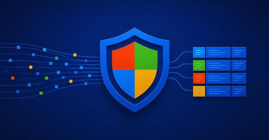
Microsoft announced today that it is accelerating its quantum-safe security roadmap, saying advances in quantum computing are bringing the need to replace today’s encryption standards sooner than previously expected.
Although today’s quantum computers cannot crack modern encryption, security researchers have warned about “harvest now, decrypt later” attacks. In these attacks, encrypted data that is stolen today is stored until future quantum computers become powerful enough to decrypt it, exposing sensitive information.
As a result, companies including Apple, Google, and Signal have begun integrating post-quantum cryptography (PQC) to replace existing public-key encryption algorithms with quantum-resistant versions.

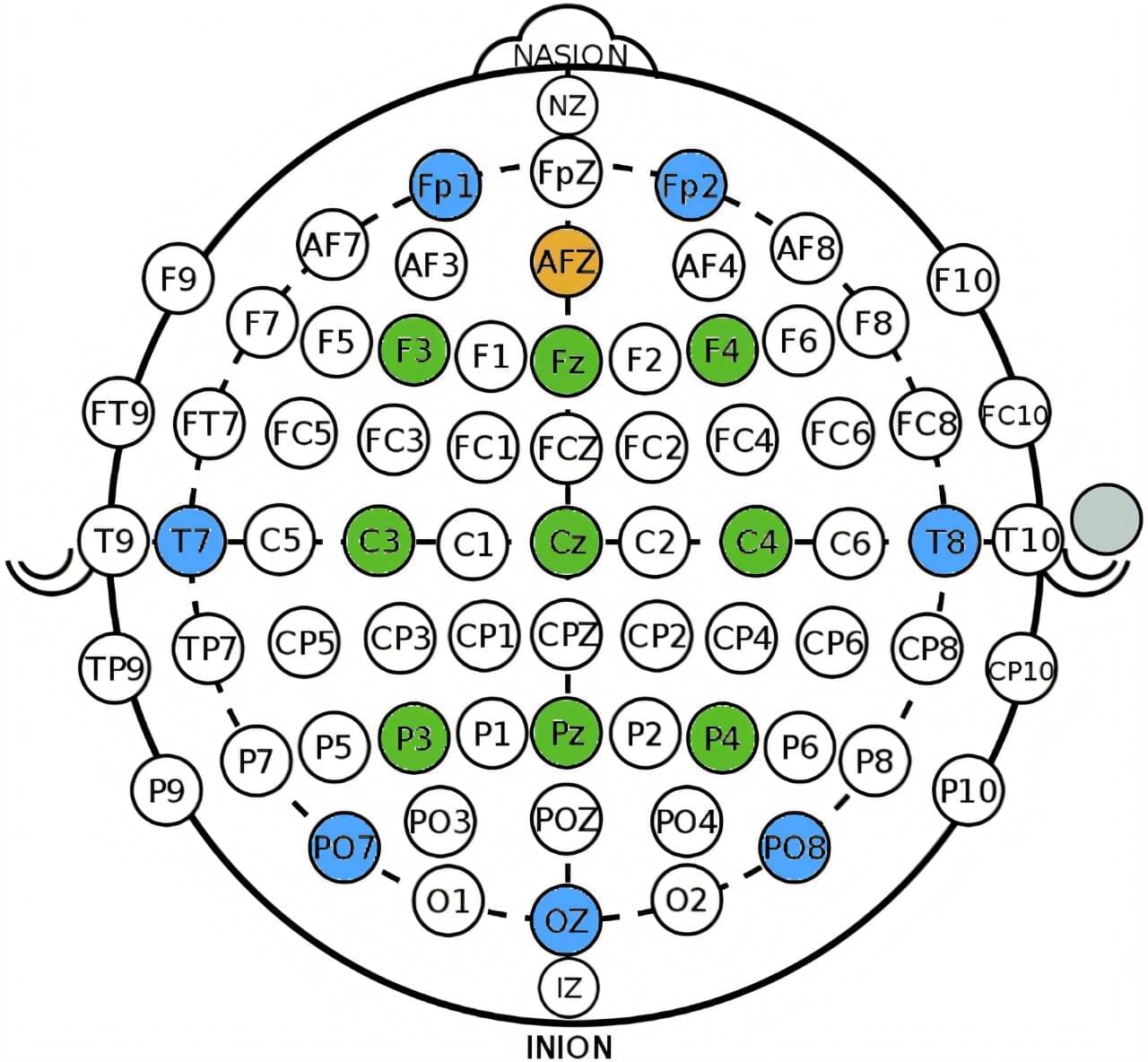
A new approach for identifying signs of hidden awareness in people who cannot speak or move after severe brain injury has been demonstrated by researchers at the University of Bath in the U.K.
The system detects patterns of brain activity through a wearable headset using an advanced application of brain-computer interface (BCI) technology.
Across multiple experimental sessions, the researchers uncovered signs of consciousness that were previously undetected in unresponsive patients.