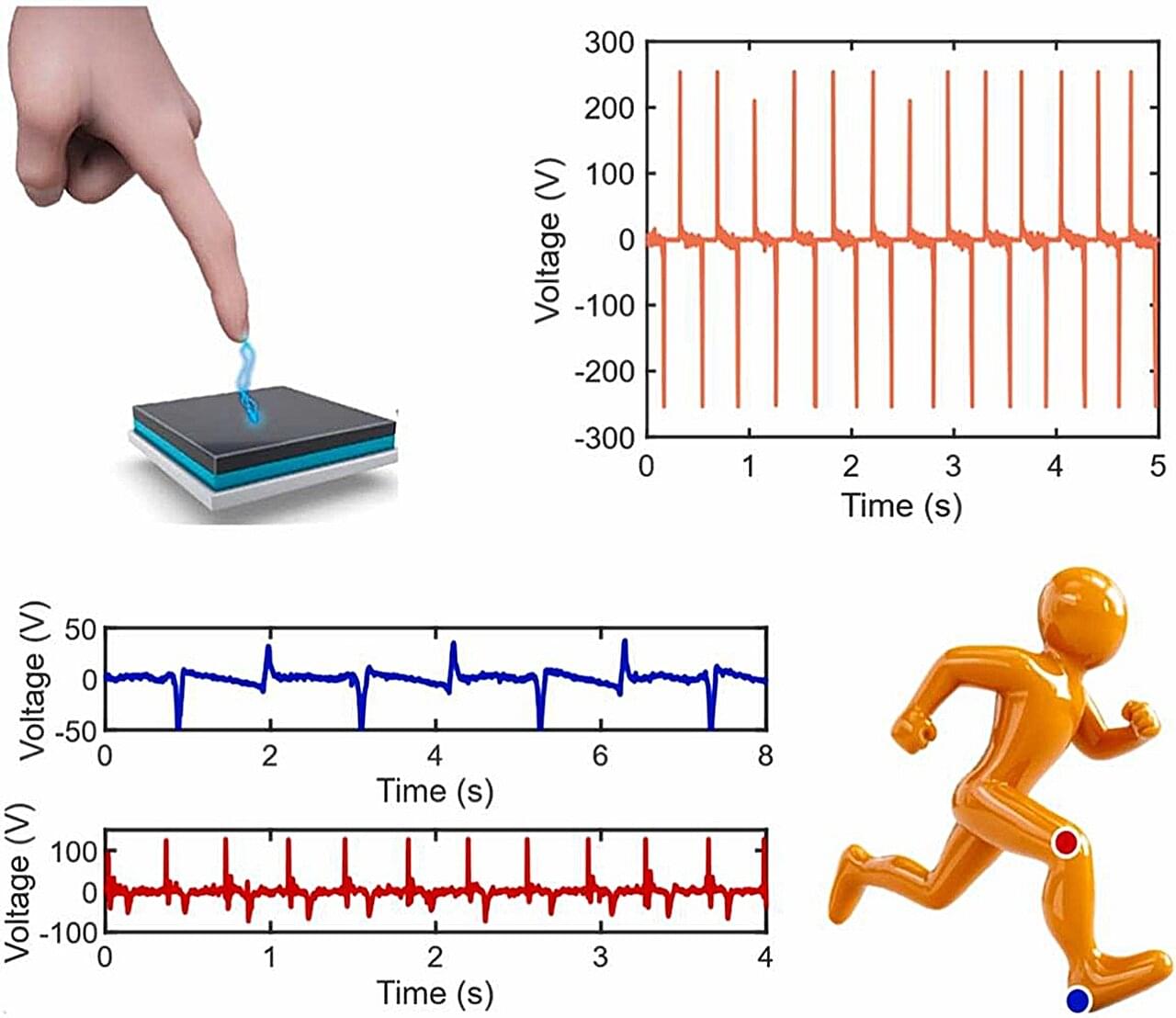
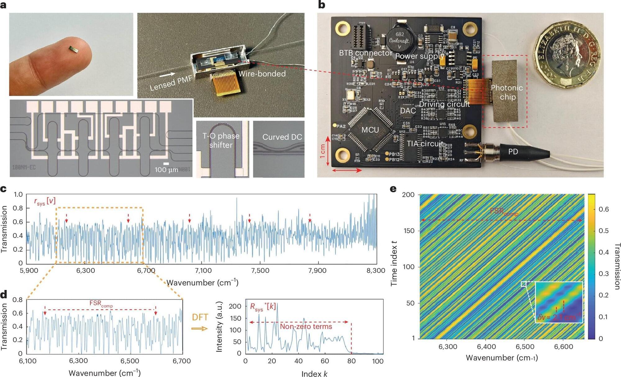
Researchers at Boise State University have developed a novel, environmentally friendly triboelectric nanogenerator (TENG) that is fully printed and capable of harvesting biomechanical and environmental energy while also functioning as a real-time motion sensor. The innovation leverages a composite of Poly (vinyl butyral-co-vinyl alcohol-co-vinyl acetate) (PVBVA) and MXene (Ti3C2Tx) nanosheets, offering a sustainable alternative to conventional TENGs that often rely on fluorinated polymers and complex fabrication.
TENGs are innovative energy-harvesting devices that convert mechanical energy into electricity using the triboelectric effect. They were invented by Prof. Zhong Lin Wang of the Georgia Institute of Technology and generate power through contact and motion between materials, making them ideal for applications like wearable electronics, IoT sensors, and self-powered devices.
This work, published in the journal Nano Energy and led by Ph.D. student Ajay Pratap under the supervision of Prof. David Estrada of the Micron School of Materials Science and Engineering at Boise State University, showcases how additive manufacturing can produce high-performance, skin-compatible, and flexible devices for real-world applications in energy harvesting, wearables electronics, and human-machine interaction.
