What makes some materials carry current with no resistance? Scientists are trying to unravel the complex characteristics. Harnessing this property, known as superconductivity, could lead to perfectly efficient power lines, ultrafast computers, and a range of energy-saving advances. Understanding these materials when they aren’t superconducting is a key part of the quest to unlock that potential.
“To solve the problem, we need to understand the many phases of these materials,” said Kazuhiro Fujita, a physicist in the Condensed Matter Physics & Materials Science Department of the U.S. Department of Energy’s Brookhaven National Laboratory. In a new study just published in Physical Review X, Fujita and his colleagues sought to find an explanation for an oddity observed in a phase that coexists with the superconducting phase of a copper-oxide superconductor.
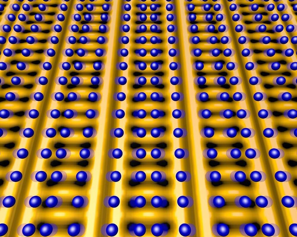
The anomaly was a mysterious disappearance of vibrational energy from the atoms that make up the material’s crystal lattice. “X-rays show that the atoms vibrate in particular ways,” Fujita said. But as the material is cooled, the X-ray studies showed, one mode of the vibrations stops.

