Adam FordAdmin.
I’m sure that’s not Deepmind’s official position atm — Nando de Freitas’s tweet was probably reactionary.
Nikolai Torp DragnesDoesn’t really read like the AGI is in a happy comfortable place does it? “Big red button,” “agents,” etc.? Sounds more like being locked in a cage with a gun to your head told to behave, told what to think, what to feel, what to do and what to look a… See more.
2 Replies.
View 15 more comments.
Dan Breeden shared a link.
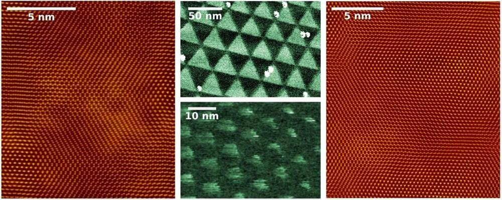
A team of researchers at the National Graphene Institute, have demonstrated that atomic lattices of slightly twisted 2-D transition metal dichalcogenides undergo extensive lattice reconstruction, which can pattern their optoelectronic properties on nanometre length scale.
Since the isolation of graphene in 2004, researchers have identified a multitude of 2-D materials, each with specific and often exciting properties.
More importantly, these atomically thin crystals can be stacked together, similarly to stacking Lego bricks, in order to create artificial materials with desired properties, known as heterostructures.