A four-year study will help develop AI software that will speed up the process of matching donated kidneys with patients in need, especially those not at the top of the transplant list.


The breakthrough came in an impossibly small slice of time, less than it takes a beam of light to move an inch. In that tiny moment, nuclear fusion as an energy source went from far-away dream to reality. The world is now grappling with the implications of the historic milestone. For Arthur Pak and the countless other scientists who’ve spent decades getting to this point, the work is just beginning.
Pak and his colleagues at Lawrence Livermore National Laboratory are now faced with a daunting task: Do it again, but better—and bigger.
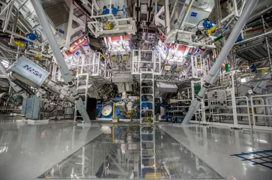
That means perfecting the use of the world’s largest laser, housed in the lab’s National Ignition Facility that science-fiction fans will recognize from the film “Star Trek: Into Darkness,” when it was used as a set for the warp core of the starship Enterprise. Just after 1 a.m. on Dec. 5, the laser shot 192 beams in three carefully modulated pulses at a cylinder containing a tiny diamond capsule filled with hydrogen, in an attempt to spark the first fusion reaction that produced more energy than it took to create. It succeeded, starting the path toward what scientists hope will someday be a new, carbon-free power source that will allow humans to harness the same source of energy that lights the stars.

Instead, this nimble satellite will punch hugely above its weight and try to track down one of the most elusive and mysterious substances in the universe: dark matter. This is the term given to the hypothetical invisible matter that is thought to be more abundant than normal matter and has a similar gravitational effect on its surroundings.
The mission is classified as fast (F), which means it is smaller, more focused, and has a quicker turnaround (less than 10 years to launch) than other types of ESA missions. The agency’s previous F-mission, selected in 2019, is called the Comet Interceptor. Already parked at a stable point in the Solar System, this probe is waiting for a comet to show up and fly by it, something that’s due to happen around the time that Arrakhis launches in the early 2030s.
Since dark matter still eludes detection, the mission will target sources of light that are sensitive to it. We expect normal matter — the stuff that actually emits light, such as stars in galaxies — to move primarily under the influence of dark matter, which is more abundant.

Researchers at Vienna University of Technology have discovered why sometimes spectacular micro-explosions occur and other times ultra-thin layers of material remain almost intact when charged particles are shot through them.
It may seem like magic that some materials can withstand being shot through with fast, electrically charged ions without exhibiting holes afterward. This phenomenon, which would be impossible at the macroscopic level, becomes possible at the level of individual particles. However, not all materials exhibit this behavior. In recent years, various research groups have conducted experiments with varying results.
Vienna University of Technology researchers have been able to provide a detailed explanation for why some materials are perforated while others are not. This is of particular interest in the processing of thin membranes, which are designed to have tailor-made nano-pores that can trap, hold, or allow specific atoms or molecules to pass through.

Sepsis is a life-threatening condition arising from the body’s overreactive response against an infection, leading it to injure its own tissues and organs. The first known reference to “sepsis” dates back more than 2,700 years, when the Greek poet Homer used it as a derivative of the word “sepo,” meaning “I rot.”
Despite dramatic improvements in understanding the immunological mechanisms behind sepsis, it still remains a major medical concern, affecting 750,000 people in the U.S. and nearly 50 million people globally each year. Sepsis accounted for 11 million deaths worldwide in 2017, and is the most expensive medical condition in the U.S., costing over tens of billions of dollars annually.
We are researchers who study how certain types of bacteria interact with cells during infections. We wanted to understand exactly how an overreactive immune response can result in detrimental and even lethal effects like sepsis. In our research, newly published in Science Immunology, we discovered the cells and molecules that potentially trigger death from sepsis.

A comet that only orbits the sun once every 50,000 years is expected to be visible from Earth with the naked eye. The last time the comet visited, the Sahara desert was wet and fertile, Neanderthals and woolly mammoths still walked the Earth, and humans were—as far as we know—yet to reach North America.
C/2022 E3 (ZTF) was first spotted by the Zwicky Transient Facility (ZTF) on March 2, 2022, and is set to reach its closest point to the sun, or perihelion, on January 12, 2023. ZTF is an astronomical survey conducted by the Palomar Observatory in California.
Comets are “cosmic snowballs” made up of frozen gases, dust and rock that orbit the sun. As they approach our star, these fragile constructs are blasted with increasing amounts of radiation, a process that can produce two vast tails of gas and dust.

Buzzy products like ChatGPT and DALL-E 2 will have to turn a profit eventually.
