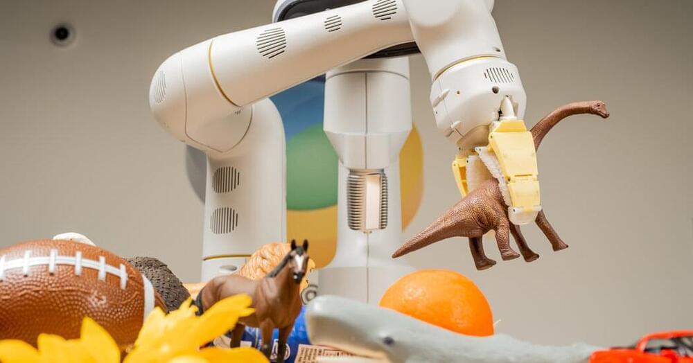
Electronics that can bend, stretch and repair themselves could potentially work in applications ranging from tougher robots to smart clothes.




Google career certificates are no longer just an alternative to college — they’re also now a way for college students to boost their earning potential, while lowering the cost of obtaining a degree.
The challenge: On average, people with bachelor’s degrees earn $27,000 more per year than people whose highest level of education is a high school diploma.
However, students can expect to spend thousands or tens of thousands of dollars per year earning their degrees through a traditional four-year program, and about two-thirds of students end up taking out loans to help pay that cost.
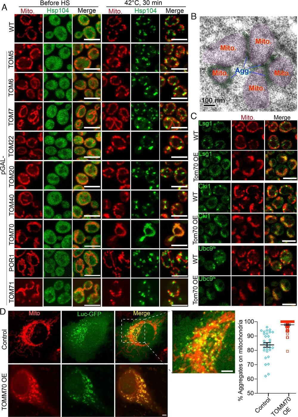
Eukaryotes organize cellular contents into membrane-bound organelles and membrane-less condensates, for example, protein aggregates. An unsolved question is why the ubiquitously distributed proteins throughout the cytosol give rise to spatially localized protein aggregates on the organellar surface, like mitochondria. We report that the mitochondrial import receptor Tom70 is involved in the localized condensation of protein aggregates in budding yeast and human cells. This is because misfolded cytosolic proteins do not autonomously aggregate in vivo; instead, they are recruited to the condensation sites initiated by Tom70’s substrates (nascent mitochondrial proteins) on the organellar membrane using multivalent hydrophobic interactions. Knocking out Tom70 partially impairs, while overexpressing Tom70 increases the formation and association between cytosolic protein aggregates and mitochondria. In addition, ectopic targeting Tom70 and its substrates to the vacuole surface is able to redirect the localized aggregation from mitochondria to the vacuolar surface. Although other redundant mechanisms may exist, this nascent mitochondrial proteins-based initiation of protein aggregation likely explains the localized condensation of otherwise ubiquitously distributed molecules on the mitochondria. Disrupting the mitochondrial association of aggregates impairs their asymmetric retention during mitosis and reduces the mitochondrial import of misfolded proteins, suggesting a proteostasis role of the organelle-condensate interactions.

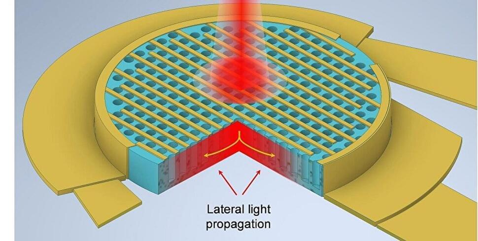
Photonic systems are quickly gaining traction in many emerging applications, including optical communications, lidar sensing, and medical imaging. However, the widespread adoption of photonics in future engineering solutions hinges on the cost of manufacturing photodetectors, which, in turn, largely depends on the kind of semiconductor utilized for the purpose.
Traditionally, silicon (Si) has been the most prevalent semiconductor in the electronics industry, so much so that most of the industry has matured around this material. Unfortunately, Si has a relatively weak light absorption coefficient in the near-infrared (NIR) spectrum compared to those of other semiconductors such as gallium arsenide (GaAs).
Because of this, GaAs and related alloys thrive in photonic applications, but are incompatible with the traditional complementary metal-oxide-semiconductor (CMOS) processes used in the production of most electronics. This leads to a drastic increase in their manufacturing costs.

No, oxygen didn’t catalyze the swift blossoming of Earth’s first multicellular organisms. The result defies a 70-year-old assumption about what caused an explosion of oceanic fauna hundreds of millions of years ago.
Between 685 and 800 million years ago, the Avalon explosion — a forerunner era of the more famed Cambrian explosion — marked the emergence of multicellular organisms in Earth’s oceans. Prior to this era, the world was dominated by single-celled amoeba, algae, and bacteria for over 2 billion years. The Avalon explosion saw a sudden surge in biodiversity, with sea sponges and other complex multicellular organisms replacing their simpler, single-celled counterparts.
Previously, it was postulated that this significant leap in evolutionary complexity was triggered by increased oxygen levels. However, this is being disproved by recent research by the University of Copenhagen, in collaboration with the Woods Hole Oceanographic Institute, the University of Southern Denmark, and Lund University, among others.

New research published in Telematics and Informatics provides evidence that the fulfillment of basic psychological needs through technology use is linked to changes in attitudes towards artificial intelligence over time. The findings indicate that self-determination, particularly feelings of competence and relatedness, plays a crucial role in shaping both negative and positive attitudes towards this emerging technology.
“We live in a world where artificial intelligence (AI) is becoming more common and accessible than ever. People’s attitudes towards AI will most certainly have a huge effect on how fast and widely AI can spread in society and how the development of AI will turn out,” said study author Jenna Bergdahl, a researcher at the Emerging Technologies Lab at Tampere University.
“As a researcher, I work in the Emerging Technologies Lab at Tampere University, where we are particularly interested in the new technological forms of life that constantly challenge and transform human and post-human living. Two projects from the Emerging Technologies Lab, called UrbanAI and Self & Technology, are focusing especially on artificial intelligence in society and conducting cross-national social psychological research on human-technology interaction.”