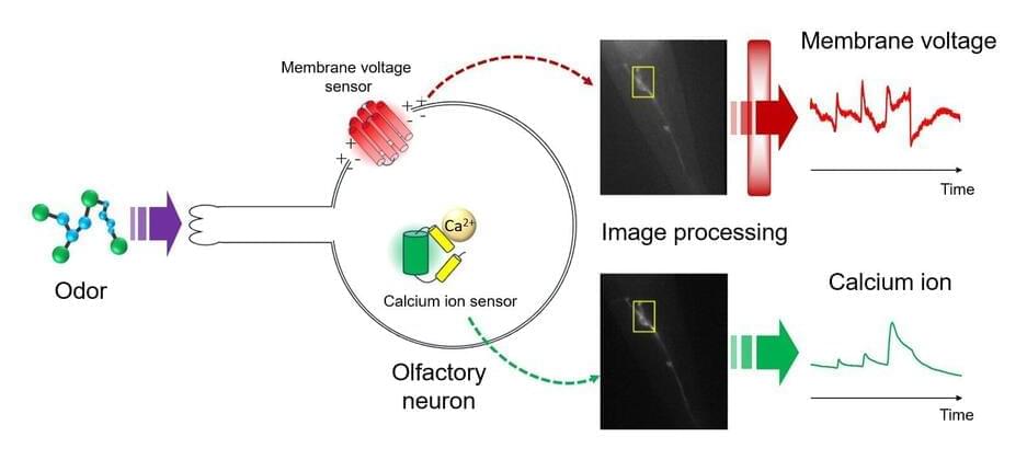
Researchers from Kyushu University have developed an innovative technique to non-invasively measure two key signals, membrane voltage and intracellular calcium levels, at the same time, in neurons of awake animals. This new method offers a more complete understanding of how neurons function, revealing that these two signals encode different information for sensory stimuli. The research was published in Communications Biology on September 16, 2024.
Neurons are cells that act as the brain’s fundamental building blocks, transmitting information through electrical signals. When a neuron receives a stimulus, changes in membrane voltage (the electrical charge across the neuron cell membrane) trigger the neuron to activate, causing rapid changes in membrane voltage to propagate along the neuron as an electrical signal. These changes in membrane voltage then lead to changes in intracellular calcium (calcium levels inside neurons).
Historically, measuring membrane voltage has involved invasive techniques using electrodes. As a non-invasive alternative, scientists have developed techniques to measure calcium activity using fluorescent proteins that are sensitive to calcium ions as sensors, providing an indirect proxy for neuron activity. However, these different methods mean that the two signals have almost always been studied separately, making it challenging to understand how they interact in real-time and to identify their distinct functions in living animals.


