Archive for the ‘nanotechnology’ category: Page 273
Sep 15, 2016
Elon Musk has some really strange ideas about connecting computers to your brain
Posted by Karen Hurst in categories: computing, Elon Musk, nanotechnology, neuroscience, robotics/AI
This is not that far fetch especially when we have seen DARPA’s efforts around BMI, the nanobot technology being experimented on to enable BMI, stent technology as well that is being looked at for BMI, etc. which all leads us into the concept of superhumans.
“Humans are so slow” says Elon Musk, so let’s become AI-human symbiotes instead.
Sep 15, 2016
Carbon-coated iron catalyst structure could lead to more-active fuel cells
Posted by Karen Hurst in categories: nanotechnology, particle physics, transportation
Abstract: Fuel cells have long held promise as power sources, but low efficiency has created obstacles to realizing that promise. Researchers at the University of Illinois and collaborators have identified the active form of an iron-containing catalyst for the trickiest part of the process: reducing oxygen gas, which has two oxygen atoms, so that it can break apart and combine with ionized hydrogen to make water. The finding could help researchers refine better catalysts, making fuel cells a more energy- and cost-efficient option for powering vehicles and other applications.
Led by U. of I. chemistry professor Andrew Gewirth, the researchers published their work in the journal Nature Communications.
Iron-based catalysts for oxygen reduction are an abundant, inexpensive alternative to catalysts containing precious metals, which are expensive and can degrade. However, the process for making iron-containing catalysts yields a mixture of different compounds containing iron, nitrogen and carbon. Since the various compounds are difficult to separate, exactly which form or forms behave as the active catalyst has remained a mystery to researchers. This has made it difficult to refine or improve the catalyst.
Sep 15, 2016
“Hairy” Nanorods Offer Simpler Production Process
Posted by Karen Hurst in categories: materials, nanotechnology
Georgia Tech researchers have developed a new strategy for crafting one-dimensional cellulose nanorods using a wide range of precursor materials.
Sep 15, 2016
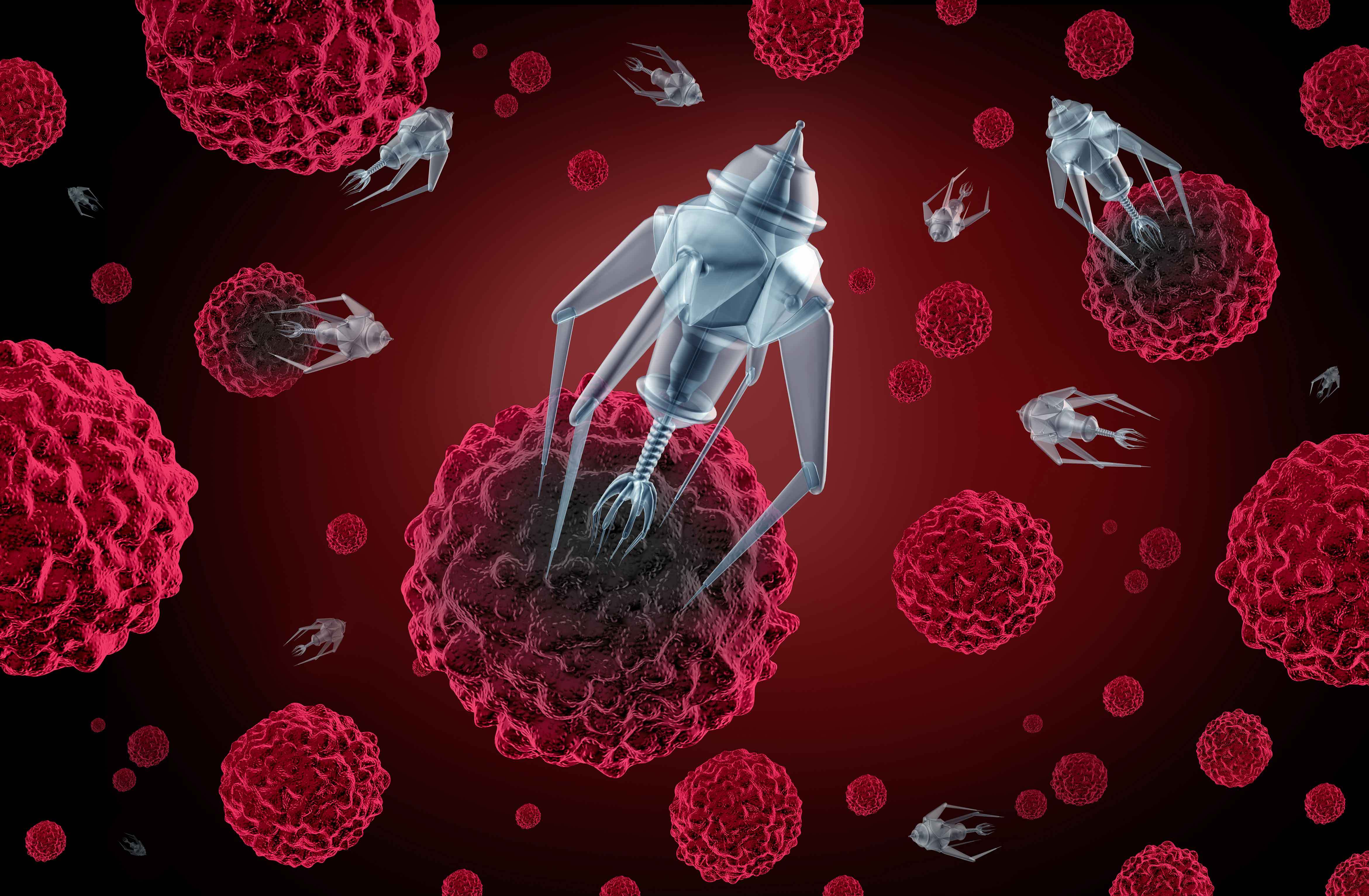
Meet the nanobots that could combat cancer
Posted by Karen Hurst in categories: biotech/medical, nanotechnology
An international team have developed nanobots that travel in the bloodstream and tackle cancer from the inside.
Sep 15, 2016
Your Thoughts Could Activate a Tiny Robot Inside Your Own Brain
Posted by Karen Hurst in categories: health, nanotechnology, neuroscience, robotics/AI
Hmmm.
For the first time, Israeli researchers have developed a system that lets a human use brain waves to control nanobots in a cockroach. How could that help your health?
Sep 15, 2016
Levitating nanoparticle improves ‘torque sensing’
Posted by Karen Hurst in categories: nanotechnology, particle physics, quantum physics
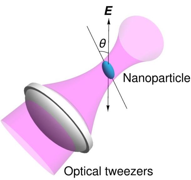
Researchers have levitated a tiny nanodiamond particle with a laser in a vacuum chamber, using the technique for the first time to detect and measure its “torsional vibration,” an advance that could bring new types of sensors and studies in quantum mechanics.
The experiment represents a nanoscale version of the torsion balance used in the classic Cavendish experiment, performed in 1798 by British scientist Henry Cavendish, which determined Newton’s gravitational constant. A bar balancing two lead spheres at either end was suspended on a thin metal wire. Gravity acting on the two weights caused the wire and bar to twist, and this twisting — or torsion — was measured to calculate the gravitational force.
In the new experiment, an oblong-shaped nanodiamond levitated by a laser beam in a vacuum chamber served the same role as the bar, and the laser beam served the same role as the wire in Cavendish’s experiment.
Sep 14, 2016
Scientists develop revolutionary heart attack sensor
Posted by Karen Hurst in categories: biotech/medical, genetics, nanotechnology
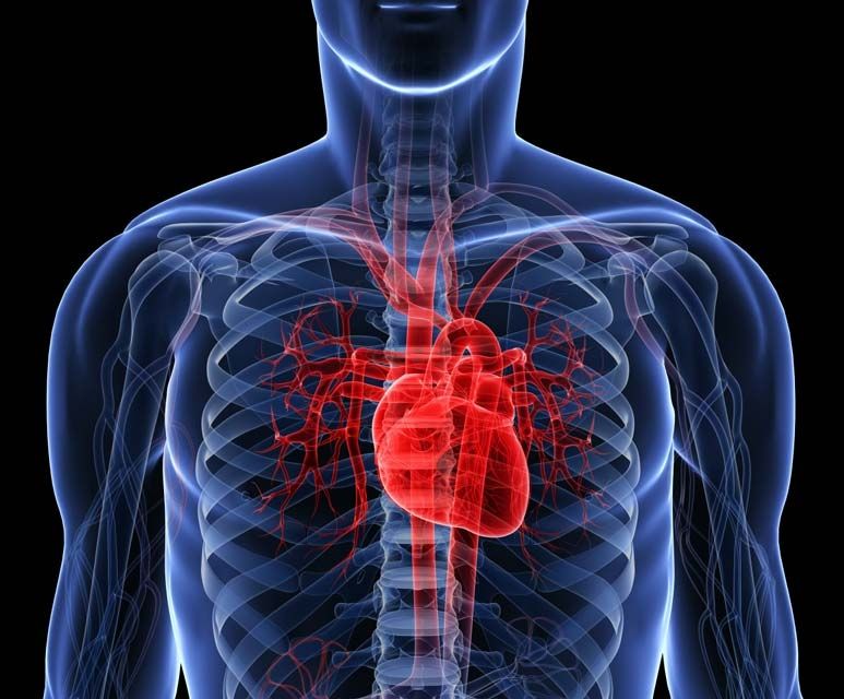 An international collaboration of scientists involving a team of researchers at Manchester led by Dr. David J. Lewis has developed a tiny electric sensor, which could potentially improve patient survival rates by telling doctors if a person has had a heart attack.
Cardiovascular diseases account for around 30 per cent of adult deaths in the 30–70 year age group, which is greater than the combined deaths from all types of cancer. The ability to diagnose cardiac disease is therefore of utmost concern to doctors. When someone has a heart attack, certain chemicals are released into their bloodstream in elevated amounts, and blood tests are therefore the key to diagnosis.
Lewis, from Manchester’s School of Materials, has worked with his colleagues and a team at India’s Institute of Nano Science and Technology (INST) since 2014 to develop a nanoscale sensor made from ‘few-layer black phosphorus’, a new 2D material, which was coated in Deoxyribonucleic Acid (DNA)/genetic material. The immobilised DNA binds to a chemical called myoglobin, which increases in blood plasma after a heart attack and can be detected and measured by a simple electrical test. This could have a major impact, as it is potentially the most rapid, sensitive, selective and accurate method currently available to detect if someone has elevated levels of myoglobin – the measurement of which is one of the methods used in hospitals to check if someone has suffered a heart attack. The researchers predict that its eventual introduction into the clinic could potentially improve patient survival rates after an attack.
Continue reading “Scientists develop revolutionary heart attack sensor” »
Sep 14, 2016
Journey to the Centre of the Cell: Nano-Rods and Worms Wriggle Best
Posted by Karen Hurst in categories: biotech/medical, nanotechnology, transportation
Interesting read.
When it comes to delivering drugs, nanoparticles shaped like rods and worms are the best bet for making the daunting journey to the centre of a cell, new Australian research suggests.
A new study published in Nature Nanotechnology has answered a long-standing question that could lead to the design of better drug delivery vehicles: how nanoparticle shape affects the voyage through the cell.
Continue reading “Journey to the Centre of the Cell: Nano-Rods and Worms Wriggle Best” »
Sep 14, 2016
UCLA chemists report new insights about properties of matter at the nanoscale
Posted by Karen Hurst in categories: chemistry, nanotechnology
UCLA’s new method to smaller molecule machines.
UCLA nanoscience researchers have determined that a fluid that behaves similarly to water in our day-to-day lives becomes as heavy as honey when trapped in a nanocage of a porous solid, offering new insights into how matter behaves in the nanoscale world.
“We are learning more and more about the properties of matter at the nanoscale so that we can design machines with specific functions,” said senior author Miguel García-Garibay, dean of the UCLA Division of Physical Sciences and professor of chemistry and biochemistry.
Continue reading “UCLA chemists report new insights about properties of matter at the nanoscale” »
