Archive for the ‘nanotechnology’ category: Page 248
May 6, 2017
Kurzweil: By 2030, Nanobots Will Flow Throughout Our Bodies
Posted by Simon Waslander in categories: biological, nanotechnology, neuroscience, Ray Kurzweil, wearables

Another futurist, Dave Evans, founder and CTO of Silicon Valley stealth startup Stringify, gave his thoughts about Kurzweil’s nanobot idea in an interview with James Bedsole on February.
Evans explained that he thinks such a merging of technology and biology isn’t at all farfetched. In fact, he described three stages as to how this will occur: the wearable phase (where we are today), the embeddable phase (where we’re headed, with neural implants and such), and the replaceable phase.
Continue reading “Kurzweil: By 2030, Nanobots Will Flow Throughout Our Bodies” »
Apr 15, 2017
Ray Kurzweil interviews the Father of Nanotechnology Eric Drexler
Posted by Simon Waslander in categories: computing, nanotechnology, Ray Kurzweil, solar power, sustainability

https://www.youtube.com/watch?v=gjIm9yIm0zo
Unimaginable Radical Abundance:
Yesterday I took the time to read chapter 11 of Eric Drexler’s book Radical Abundance as to get a glimpse of what might be possible with Atomically Precise Manufacturing (APM). I highly recommend the book.
Continue reading “Ray Kurzweil interviews the Father of Nanotechnology Eric Drexler” »
Apr 14, 2017
Graphene-oxide sieve turns seawater into drinking water
Posted by Sean Brazell in categories: nanotechnology, transportation

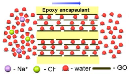
Schematic illustrating the direction of ion/water permeation along graphene planes (credit: J. Abraham et al./ Nature Nanotechnology)
Continue reading “Graphene-oxide sieve turns seawater into drinking water” »
Apr 12, 2017
Silver Circuits On Foil Allow Curved Touchscreens
Posted by Roman Mednitzer in categories: mobile phones, nanotechnology
Microscopically fine conductor paths are required on the surfaces of smartphone touchscreens. At the edges of the appliances, these microscopic circuit paths come together to form larger connective pads. Until now, these different conductive paths had to be manufactured in several steps in time-consuming processes. With photochemical metallization, this is now possible in one single step on flexible substrates. The process has several benefits: It is fast, flexible, variable in size, inexpensive and environmentally friendly. Additional process steps for post-treatment are not necessary.
For the new process, the foils are coated with a photoactive layer of metal oxide nanoparticles. “After that, we apply a colorless, UV-stable silver compound,” Peter William de Oliveira, head of optical materials, explains. By irradiation of this sequence of layers, the silver compound disintegrates on the photoactive layer and the silver ions are reduced to form metallic, electrically conductive silver. In this way, paths of varying sizes down to the smallest size of a thousandth of a millimeter can be achieved.
This basic principle allows conductive paths to be created individually. “There are different possibilities we can use depending on the requirements: Writing conductive paths using UV lasers is particularly suitable for the initial customized prototype manufacture and testing a new design of the conductive path. However, for mass production, this method is too time-consuming,” de Oliveira explains.
Continue reading “Silver Circuits On Foil Allow Curved Touchscreens” »
Apr 4, 2017
Nanofabrication Enables “Particle-Accelerator-on-a-Chip” Technology
Posted by Klaus Baldauf in categories: biotech/medical, computing, nanotechnology
The key to this all working is the design of the nanostructures. If you just have a laser in free space, the particle will just oscillate back and forth, pushing it one way and then the other. It won’t ever gain in total energy. So you need some kind of structure that channels or modulates the fields in such a way that the particle will travel along mainly the peaks of the electromagnetic wave and not into the troughs so that it gets kicks but not deceleration.
In all of the experiments done so far, England explains that the particles are basically filling the whole wave, occupying and seeing both the peaks and troughs. This results in some particles being accelerated while others get decelerated.
“In the future, as one of the next experimental steps what we want is to bunch the particles to make very short little packets of particles that are spaced at exactly the right distance between the peaks so that they will ride only on the peaks,” says England. “So you can think of it as like… ocean waves, and you want your surfers to be positioned only on the peaks of the waves and not in the troughs.”
Continue reading “Nanofabrication Enables ‘Particle-Accelerator-on-a-Chip’ Technology” »
Mar 21, 2017
The world’s most efficient and environment-friendly solar cells
Posted by Simon Waslander in categories: nanotechnology, solar power, sustainability
In the future, solar cells can become twice as efficient by employing a few smart little nano-tricks.
Researchers are currently developing the environment-friendly solar cells of the future, which will capture twice as much energy as the cells of today. The trick is to combine two different types of solar cells in order to utilize a much greater portion of the sunlight.
“These are going to be the world’s most efficient and environment-friendly solar cells. There are currently solar cells that are certainly just as efficient, but they are both expensive and toxic. Furthermore, the materials in our solar cells are readily available in large quantities on Earth. That is an important point,” says Professor Bengt Svensson of the Department of Physics at the University of Oslo (UiO) and Centre for Materials Science and Nanotechnology (SMN).
Continue reading “The world’s most efficient and environment-friendly solar cells” »
Mar 19, 2017
Nanoscale logic machines go beyond binary computing
Posted by Shailesh Prasad in categories: computing, information science, nanotechnology, particle physics
(Phys.org)—Scientists have built tiny logic machines out of single atoms that operate completely differently than conventional logic devices do. Instead of relying on the binary switching paradigm like that used by transistors in today’s computers, the new nanoscale logic machines physically simulate the problems and take advantage of the inherent randomness that governs the behavior of physical systems at the nanoscale—randomness that is usually considered a drawback.
The team of researchers, Barbara Fresch et al., from universities in Belgium, Italy, Australia, Israel, and the US, have published a paper on the new nanoscale logic machines in a recent issue of Nano Letters.
“Our approach shows the possibility of a new class of tiny analog computers that can solve computationally difficult problems by simple statistical algorithms running in nanoscale solid-state physical devices,” coauthor Francoise Remacle at the University of Liege told Phys.org.
Mar 15, 2017
New nano-implant could one day help restore sight
Posted by Klaus Baldauf in categories: biotech/medical, cyborgs, law, nanotechnology, neuroscience
A team of engineers at the University of California San Diego and La Jolla-based startup Nanovision Biosciences Inc. have developed the nanotechnology and wireless electronics for a new type of retinal prosthesis that brings research a step closer to restoring the ability of neurons in the retina to respond to light. The researchers demonstrated this response to light in a rat retina interfacing with a prototype of the device in vitro.
They detail their work in a recent issue of the Journal of Neural Engineering. The technology could help tens of millions of people worldwide suffering from neurodegenerative diseases that affect eyesight, including macular degeneration, retinitis pigmentosa and loss of vision due to diabetes.
Despite tremendous advances in the development of retinal prostheses over the past two decades, the performance of devices currently on the market to help the blind regain functional vision is still severely limited—well under the acuity threshold of 20/200 that defines legal blindness.
Mar 14, 2017
IBM Has Devised a Way to “Grow” Computer Chips
Posted by Bryan Gatton in categories: computing, nanotechnology
In Brief
- Scientists have devised a way, inspired by nature, of coaxing carbon nanotubes to build themselves into structures that could be used to replace silicon chips.
- The successful implementation of this technology could lead to faster than silicon computer chips along with bendable electronics.
Traditionally, computer microchips are made of the semiconductor silicon. Silicon is turned into wafers where complex circuitry is carved—but there’s a limit to this complexity and to the chips’ processing capacity, and it’s coming soon.
Scientist from IBM are ushering in a revolution of microchip design by seeking to use carbon nanotubes. The researchers theorize that these nanotube chips could use less electricity, and be six to ten times faster than silicon-based ones.

