Menu

Blog

Archive for the ‘nanotechnology’ category: Page 22

Aug 1, 2024

Nonreciprocal Interactions Go Nonlinear: How Nanoparticles Are Changing the Rules of Physics

Posted by in categories: nanotechnology, physics

Using two optically trapped glass nanoparticles, researchers observed a novel collective Non-Hermitian and nonlinear dynamic driven by nonreciprocal interactions. This contribution expands traditional optical levitation with tweezer arrays by incorporating the so-called non-conservative interactions. Their findings, supported by an analytical model developed by collaborators from Ulm University and the University of Duisburg-Essen, were recently published in Nature Physics.

Understanding Nonreciprocal Interactions

Fundamental forces like gravity and electromagnetism are reciprocal, meaning two objects either attract or repel each other. However, for some more complex interactions arising in nature, this symmetry is broken and some form of nonreciprocity exists. For example, the interaction between a predator and a prey is inherently nonreciprocal as the predator wants to catch (is attracted to) the prey and the latter wants to escape (is repelled).

Jul 31, 2024

Researchers identify unique phenomenon in Kagome metal

Posted by in categories: nanotechnology, quantum physics

In traditional Japanese basket-weaving, the ancient “Kagome” design seen in many handcrafted creations is characterized by a symmetrical pattern of interlaced triangles with shared corners. In quantum physics, the Kagome name has been borrowed by scientists to describe a class of materials with an atomic structure closely resembling this distinctive lattice pattern.

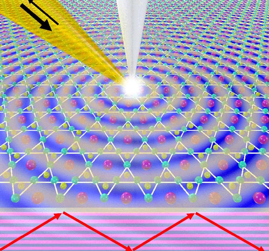
Since the latest family of Kagome metals was discovered in 2019, physicists have been working to better understand their properties and potential applications. A new study led by Florida State University Assistant Professor of Physics Guangxin Ni focuses on how a particular Kagome metal interacts with light to generate what are known as plasmon polaritons — nanoscale-level linked waves of electrons and electromagnetic fields in a material, typically caused by light or other electromagnetic waves.

The work was published in Nature Communications (“Plasmons in the Kagome metal CsV 3 Sb 5 ”).

Jul 31, 2024

The New Gods of Weather Can Make Rain on Demand—or So They Want You to Believe

Posted by in categories: nanotechnology, transportation

In a gold-trimmed command center on the outskirts of Abu Dhabi, scientists are seeking to wring moisture from desert skies. But will all their extravagant cloud-seeding tech—planes that sprinkle nanomaterials, lasers that scramble the atmosphere—really work at scale?

Jul 31, 2024

Newly discovered sheets of nanoscale ‘cubes’ make excellent catalysts

Posted by in categories: nanotechnology, particle physics

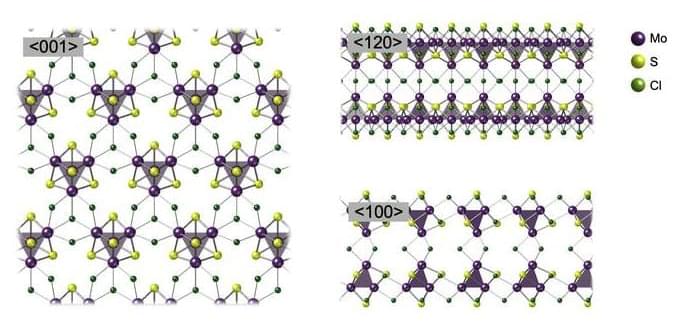
Researchers from Tokyo Metropolitan University have created sheets of transition metal chalcogenide “cubes” connected by chlorine atoms. While sheets of atoms have been widely studied e.g. graphene, the team’s work breaks new ground by using clusters instead. The team succeeded in forming nanoribbons inside carbon nanotubes for structural characterization, while also forming microscale sheets of cubes which could be exfoliated and probed. These were shown to be an excellent catalyst for generating hydrogen.

The findings have been published in Advanced Materials (“Superatomic layer of cubic Mo 4 S 4 clusters connected by Cl cross-linking”).

„ and show the arrangement of the nanosheet when viewed from different directions, respectively. (Image: Tokyo Metropolitan University)

Jul 30, 2024

New, more sustainable method for manufacturing microchips and other nanoscale devices

Posted by in categories: biological, computing, nanotechnology, sustainability

Putting 50 billion transistors into a microchip the size of a fingernail is a feat that requires manufacturing methods of nanometer level precision—layering of thin films, then etching, depositing, or using photolithography to create the patterns of semiconductor, insulator, metal, and other materials that make up the tiny working devices within the chip.

The process relies heavily on solvents that carry and deposit materials in each layer—solvents that can be difficult to handle and toxic to the environment.

Now researchers led by Fiorenzo Omenetto, Frank C. Doble Professor of Engineering at Tufts, have developed a nanomanufacturing approach that uses water as the primary solvent, making it more environmentally compatible and opening the door to the development of devices that combine inorganic and biological materials.

Jul 30, 2024

Scientists ‘Mind Controlled’ Mice Remotely in Extraordinary World First

Posted by in categories: bioengineering, biotech/medical, genetics, nanotechnology, neuroscience

At the mere flick of a magnetic field, mice engineered with nanoparticle-activated ‘switches’ inside their brains were driven to feed, socialize, and act like clucky new mothers in an experiment designed to test an innovative research tool.

While ’mind control’ animal experiments are far from new, they have generally relied on cumbersome electrodes tethering the subject to an external system, which not only requires invasive surgery but also sets limits on how freely the test subject can move about.

In what is claimed to be a breakthrough in neurology, researchers from the Institute for Basic Science (IBS) in Korea have developed a method for targeting pathways in the brain using a combination of genetics, nanoparticles, and magnetic fields.

Jul 29, 2024

Researchers trap atoms, forcing them to serve as photonic transistors

Posted by in categories: computing, engineering, nanotechnology, particle physics, quantum physics, tractor beam

Researchers at Purdue University have trapped alkali atoms (cesium) on an integrated photonic circuit, which behaves like a transistor for photons (the smallest energy unit of light) similar to electronic transistors. These trapped atoms demonstrate the potential to build a quantum network based on cold-atom integrated nanophotonic circuits. The team, led by Chen-Lung Hung, associate professor of physics and astronomy at the Purdue University College of Science, published their discovery in the American Physical Society’s Physical Review X (“Trapped Atoms and Superradiance on an Integrated Nanophotonic Microring Circuit”).

“We developed a technique to use lasers to cool and tightly trap atoms on an integrated nanophotonic circuit, where light propagates in a small photonic ‘wire’ or, more precisely, a waveguide that is more than 200 times thinner than a human hair,” explains Hung, who is also a member of the Purdue Quantum Science and Engineering Institute. “These atoms are ‘frozen’ to negative 459.67 degrees Fahrenheit or merely 0.00002 degrees above the absolute zero temperature and are essentially standing still. At this cold temperature, the atoms can be captured by a ‘tractor beam’ aimed at the photonic waveguide and are placed over it at a distance much shorter than the wavelength of light, around 300 nanometers or roughly the size of a virus. At this distance, the atoms can very efficiently interact with photons confined in the photonic waveguide. Using state-of-the-art nanofabrication instruments in the Birck Nanotechnology Center, we pattern the photonic waveguide in a circular shape at a diameter of around 30 microns (three times smaller than a human hair) to form a so-called microring resonator. Light would circulate within the microring resonator and interact with the trapped atoms.”

A key aspect function the team demonstrates in this research is that this atom-coupled microring resonator serves like a ‘transistor’ for photons. They can use these trapped atoms to gate the flow of light through the circuit. If the atoms are in the correct state, photons can transmit through the circuit. Photons are entirely blocked if the atoms are in another state. The stronger the atoms interact with the photons, the more efficient this gate is.

Jul 27, 2024

Twisted carbon nanotubes could achieve significantly better energy storage than advanced lithium-ion batteries

Posted by in categories: biotech/medical, nanotechnology

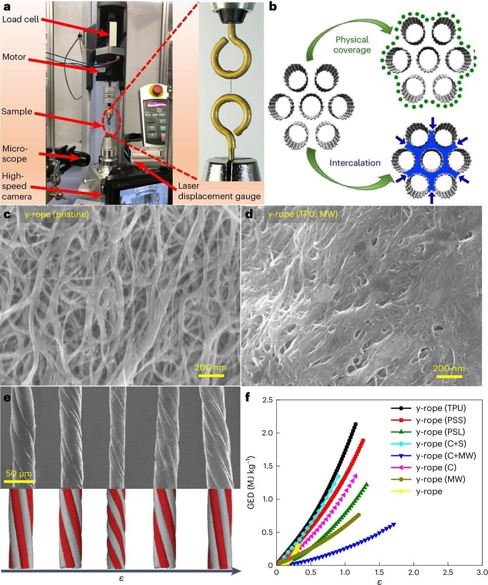
An international team of scientists, including two researchers who now work in the Center for Advanced Sensor Technology (CAST) at UMBC, has shown that twisted carbon nanotubes can store three times more energy per unit mass than advanced lithium-ion batteries. The finding may advance carbon nanotubes as a promising solution for storing energy in devices that need to be lightweight, compact, and safe, such as medical implants and sensors. The research was published recently in the journal Nature Nanotechnology.

Jul 26, 2024

Carving Out Nanostructures Beneath the Surface of Silicon

Posted by in categories: computing, nanotechnology, transportation

Modern computer chips can have features built on a nanometer scale. Until now it has been possible to form such small structures only on top of a silicon wafer, but a new technique can now create nanoscale features in a layer below the surface. The approach has promising applications in both photonics and electronics, say its inventors, and could one day enable the fabrication of 3D structures throughout the bulk of the wafer.

The technique relies on the fact that silicon is transparent to certain wavelengths of light. This means the right kind of laser can travel through the surface of the wafer and interact with the silicon below. But designing a laser that can pass through the surface without causing damage and still carry out precise nanoscale fabrication below is not simple.

Researchers from Bilkent University in Ankara, Türkiye, achieved this by using spatial light modulation to create a needlelike laser beam that gave them greater control over where the beam’s energy was deposited. By exploiting physical interactions between the laser light and the silicon, they were able to fabricate lines and planes with different optical properties that could be combined to create nanophotonic elements below the surface.

Jul 26, 2024

Novel optical nanoscopy unveils ultrafast dynamics in nanomaterials

Posted by in categories: materials, nanotechnology

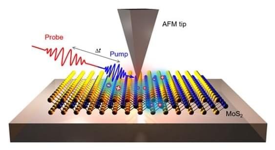
Researchers from the University of California, Berkeley have developed cutting-edge nanoscale optical imaging techniques to provide unprecedented insights into the ultrafast carrier dynamics in advanced materials. Two recent studies, published in Advanced Materials (“Transient Nanoscopy of Exciton Dynamics in 2D Transition Metal Dichalcogenides”) and ACS Photonics (“Near-Field Nanoimaging of Phases and Carrier Dynamics in Vanadium Dioxide Nanobeams”), showcase significant progress in understanding the carrier behaviors in two-dimensional and phase-change materials, with implications for next-generation electronic and optoelectronic devices.

The research team, led by Prof. Costas P. Grigoropoulos, Dr. Jingang Li, and graduate student Rundi Yang, employed a novel near-field transient nanoscopy technique to probe the behavior of materials at the nanoscale with both high spatial and temporal resolution. This approach overcomes the limitations of traditional optical methods, allowing researchers to directly visualize and analyze phenomena that were previously difficult to observe.

Schematic of the near-field transient nanoscopy. (Image: Adapted from DOI:10.1002/adma.202311568, CC BY-NC-ND 4.0)

Page 22 of 315First1920212223242526Last