Jean Housen/Wikimedia Commons.
Researchers have uncovered valuable information about how these ancient societies were organized by analyzing ancient human DNA from a site in Gurgy ‘les Noisats,’ France, dating back to 7,000 years.


A cutting-edge practice by two Vanderbilt researchers that enhances light in nanoscale structures could help in the detection of diseases like cancer.
The work by Justus Ndukaife, assistant professor of electrical engineering, and Sen Yang, a recent Ph.D. graduate from Ndukaife’s lab in Interdisciplinary Materials Science under Ndukaife, was published in Light: Science & Applications.
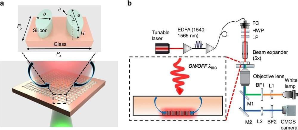
In their paper, they show how an engineered nanostructured surface—quasi-BIC dielectric metasurface—can be used to trap micro and sub-micron particles within seconds, which they say helps in the transport of analytes to biosensing surfaces. The metasurface can also serve as a sensor to detect the aggregated particles or molecules, and can be used to enhance fluorescence or Raman signals from the molecules, thereby boosting detection sensitivity, according to the researchers.

Dismantling the belief in a static universe, Edwin Hubble’s revolutionary observations in the 1920s laid the groundwork for our understanding of a continually expanding cosmos. However, we must seek to reconcile this theory with observations that are consistent with a non-expanding universe, writes Tim Anderson.
You have been taught that the universe began with a Big Bang, a hot, dense period about 13.8 billion years ago. And the reason we believe this to be true is because the universe is expanding and, therefore, was smaller in the past. The Cosmic Microwave Background is the smoking gun for the Big Bang, the result of a reionization of matter that made the universe transparent about 300–400,000 years after the Big Bang.
How did we go from Einstein modifying his equations to keep the universe static and eternal, which he called the biggest blunder of his life, to every scientist believing that the universe had a beginning in 10 years? It all started with astronomer Edwin Hubble using the most powerful telescope at the time on Mount Wilson in California. At the time, in the 1920s, scientists believed that the Milky Way galaxy was the totality of the universe. Objects in the night sky like Andromeda that we now know are galaxies were called “nebulae”.


MIT scientists and colleagues have created a simple superconducting device that could transfer current through electronic devices much more efficiently than is possible today. As a result, the new diode, a kind of switch, could dramatically cut the amount of energy used in high-power computing systems, a major problem that is estimated to become much worse.
Even though it is in the early stages of development, the diode is more than twice as efficient as similar ones reported by others. It could even be integral to emerging quantum computing technologies. The work, which is reported in the July 13 online issue of Physical Review Letters, is also the subject of a news story in Physics Magazine.
“This paper showcases that the superconducting diode is an entirely solved problem from an engineering perspective,” says Philip Moll, Director of the Max Planck Institute for the Structure and Dynamics of Matter in Germany. Moll was not involved in the work. “The beauty of [this] work is that [Moodera and colleagues] obtained record efficiencies without even trying [and] their structures are far from optimized yet.”
The stars have always held significance for humans, but it is only recently that we have begun to comprehend vast groups of them, or galaxies, in the far reaches of the universe. The Webb telescope was anticipated by everybody as a game-changer in the field of astronomy. And we knew exactly what we believed Webb would completely astound us with. However, its most recent findings have blown away the proportions of our expectations. The Webb Telescope, according to American astrophysicist Neil deGrasse Tyson, has allowed us to glimpse ghosts from the past.
Subscribe Here ➡
#Voyager #Space
Watch over 2,400 documentaries for free for 30 days AND get a free Nebula account by signing up at https://curiositystream.com/upandatom and using the code “upandatom”.
New streaming platform Nebula: https://watchnebula.com/
The Anthropic Principle and why we might live in a multiverse.
Hi! I’m Jade. Subscribe to Up and Atom for physics, math and computer science videos!
*SUBSCRIBE TO UP AND ATOM* https://www.youtube.com/c/upandatom.
Visit the Up and Atom Store.
The Big Bang theory suggests that the universe emerged out of nothing, signifying the beginning of the universe. Before this, there was nothing — no time, no space. However, what if I told you that time doesn’t exist and that the Big Bang Theory is incorrect? Recent discoveries made by the James Webb Telescope provide evidence that challenges the validity of the Big Bang Theory.