Training AI models with AI-generated synthetic content causes the quality of the models’ outputs to disintegrate, a new paper shows.


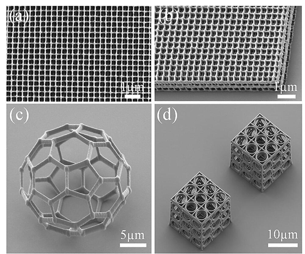
Researchers have developed an easy-to-build, low-cost 3D nanoprinting system that can create arbitrary 3D structures with extremely fine features. The new 3D nanoprinting technique is precise enough to print metamaterials as well as a variety of optical devices and components such as microlenses, micro-optical devices and metamaterials.
“Our system uses a two-step absorption process to realize 3D printing with accuracy reaching the nanometer level, which is suitable for commercial manufacturing,” said research team leader Cuifang Kuang from the Zhejiang Lab and Zhejiang University, both in China. “It can be used for a variety of applications such as printing micro or nanostructures for studying biological cells or fabricating the specialized optical waveguides used for virtual and augmented reality devices.”
Conventional high-resolution 3D nanoprinting approaches use pulsed femtosecond lasers that cost tens of thousands of dollars. In Optics Letters, Kuang and colleagues describe their new system based on an integrated fiber-coupled continuous-wave laser diode that is not only inexpensive but also easy to operate.

Rene Descartes, the father of cartesian philosophy, puts forward the relationship between sciences and especially the relation of metaphysics with other sciences through a metaphor known as the “Tree of Knowledge.” He describes knowledge as a tree and sciences are connected with each other as if they are parts of a tree. Its trunk is physics, its branches are other sciences and the fruit, which is considered to be the goal of a tree, is the science of morals. We are familiar with this metaphor and its varieties in philosophy and Sufism. In particular, it is a common metaphor to accept morals as “the fruit.” Morals, which are the intent of scientific activity, are deemed worthy of being the fruit, or the goal, by many thinkers. As a matter of fact, Ibn Arabi and Qunawi also used the same metaphor. They categorized the science of morals that is often identified with Sufism as the fruit of a tree and the goal of all human endeavors. Descartes completes his metaphor by saying that the tree’s roots are metaphysics. It is the roots that sustain a tree; the trunk, branches and fruits all depend on roots and are nourished by them, which makes the roots the most indispensable part. In this respect, this metaphor can be interpreted as a tribute to metaphysics.
While the tree of knowledge designates the place metaphysics holds among sciences, it seems to correspond with classical metaphysics, at least formally. Because the principal and subsidiary divisions of science (root and branch) are used by classical metaphysics to explain the relation of metaphysics with other sciences, the concepts of “principle and subsidiary” can be replaced by “universal and divisive,” and the meaning will not change: Metaphysics is a universal science and all other sciences serve to it as its particulars. It separates from other sciences, which examine the being from a specific angle, as metaphysics examines being qua being. Its superiority comes from this unique field of research. Because of its superior status, metaphysics is entrusted with another duty: Universal science is the most fundamental field as it certifies the principles of other sciences. The most controversial part of this assertion is whether such a superior science is possible and, if so, what method it has to attain knowledge. We will get to that, but now it is enough to state that: Despite the formal similarities, it is unlikely that Descartes could form a metaphysical understanding through this metaphor in the classical sense.
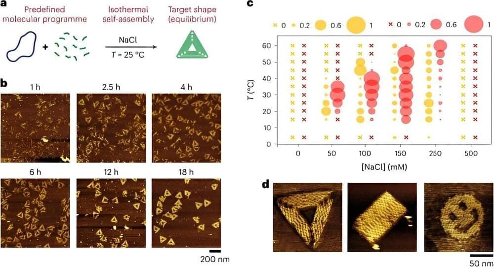
Multiple complementary DNA strands can be thermally annealed into desired entities to engineer DNA nanostructures. In a new study now published in Nature Nanotechnology, Caroline Rossi-Gendron and a team of researchers in chemistry, materials science and biology in France and Japan used a magnesium-free buffer containing sodium chloride, complex cocktails of DNA strands and proteins to self-assemble isothermally at room temperature or physiological temperature into user-defined nanostructures including nanogrids, DNA origami and single-stranded tile assemblies.
This self-assembly relied on thermodynamics, proceeding through multiple folding pathways to create highly configurable nanostructures. The method allowed the self-selection of the most stable shape in a large pool of competitive DNA strands. Interestingly, DNA origami can shift isothermally from an initially stable shape to a radically different one through an exchange of constitutive staple strands. This expanded the collection of shapes and functions obtained via isothermal self-assembly to create the foundation for adaptive nanomachines and facilitate evolutionary nanostructure discovery.
Self-assembly occurs when naturally occurring or rationally designed entities can embed necessary information to spontaneously interact and self-organize into functional superstructures of interest. Typically, synthetic self-assembled materials result from the organization of a repeating single component to create a stable supramolecular assembly containing micelles or colloidal crystals with a prescribed set of useful properties. Such constructs have limited reconfigurability, making it highly challenging to produce the desired structures.
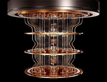
There is increasing talk of quantum computers and how they will allow us to solve problems that traditional computers cannot solve. It’s important to note that quantum computers will not replace traditional computers: they are only intended to solve problems other than those that can be solved with classical mainframe computers and supercomputers. And any problem that is impossible to solve with classical computers will also be impossible with quantum computers. And traditional computers will always be more adept than quantum computers at memory-intensive tasks such as sending and receiving e-mail messages, managing documents and spreadsheets, desktop publishing, and so on.
There is nothing “magic” about quantum computers. Still, the mathematics and physics that govern their operation are more complex and reside in quantum physics.
The idea of quantum physics is still surrounded by an aura of great intellectual distance from the vast majority of us. It is a subject associated with the great minds of the 20th century such as Karl Heisenberg, Niels Bohr, Max Planck, Wolfgang Pauli, and Erwin Schrodinger, whose famous hypothetical cat experiment was popularized in an episode of the hit TV show ‘The Big Bang Theory’. As for Schrodinger, his observations of the uncertainty principle, serve as a reminder of the enigmatic nature of quantum mechanics. The uncertainty principle holds that the observer determines the characteristics of an examined particle (charge, spin, position) only at the moment of detection. Schrödinger explained this using the theoretical experiment, known as the paradox of Schrödinger’s cat. The experiment’s worth mentioning, as it describes one of the most important aspects of quantum computing.
I am studying Noether’s theorem in field theory and I am not understanding what spacelike-surfaces mean. I will reproduce the bit of the argument below that contains the term “spacelike-sufaces” in the context I am not understanding.
There will be a conserved ccurrent for each group generator $a$. Each will result in a conserved charge (that is, an integral of motion). To see this, take in spacetime a volume unbounded in the space-like direction, but limited in time by two space-like surfaces $w_1$ and $w_2$. Integrating $\partial_{\mu} J^{\mu}_a=0$ over this volume, we get an integral over the boundary surface, composed of $w_1$, $w_2$ and the time-like boundaries supposed to be at infinity. If we now suppose the current to be zero at infinity on these boundaries, we remain with.
$$\int_{w_1}d\sigma_{\mu} J^{\mu}_a=\int_{w_2}d\sigma_{\mu} J^{


Genome editing is a powerful breeding technique that introduces mutations into specific gene sequences in genomes. For genome editing in higher plants, nucleotides for artificial nuclease (e.g. TALEN or CRISPR-Cas9) are transiently or stably introduced into the plant cells. After the introduction of mutations by artificial nucleases, it is necessary to select lines that do not contain the foreign nucleotides to overcome GMO regulation; however, there is still no widely legally authorized and approved method for detecting foreign genes in genome-edited crops. Recently, k-mer analysis based on next-generation sequencing (NGS) was proposed as a new method for detecting foreign DNA in genome-edited agricultural products. Compared to conventional methods, such as PCR and Southern hybridization, in principle, this method can detect short DNA fragments with high accuracy.
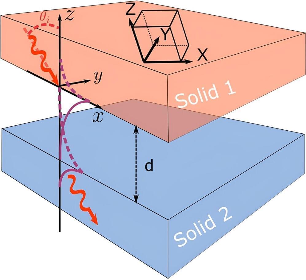
The classic film “Alien” was once promoted with the tagline “In space, no one can hear you scream.” Physicists Zhuoran Geng and Ilari Maasilta from the Nanoscience Center at the University of Jyväskylä, Finland, have demonstrated that, on the contrary, in certain situations, sound can be transmitted strongly across a vacuum region.
In a recent article published in Communications Physics they show that in some cases, a sound wave can jump or “tunnel” fully across a vacuum gap between two solids if the materials in question are piezoelectric. In such materials, vibrations (sound waves) produce an electrical response as well, and since an electric field can exist in vacuum, it can transmit the sound waves.
The requirement is that the size of the gap is smaller than the wavelength of the sound wave. This effect works not only in audio range of frequencies (Hz–kHz), but also in ultrasound (MHz) and hypersound (GHz) frequencies, as long as the vacuum gap is made smaller as the frequencies increase.

Recent research published in Nature Communications has used machine learning algorithms to find new compounds that can eliminate senescent cells [1].
Senolytics are molecules that destroy senescent cells. Only a small number of such molecules have been identified, and only two have shown efficacy in clinical trials: dasatinib and quercetin in combination [2]. One of the biggest challenges is that senolytics often only work against specific types of cells. Additionally, some senolytics may work well for one cell type while being toxic to other, non-senescent cell types [3].
There is also a group of senolytics that are used in cancer therapies. However, most of them target pathways that are mutated in cancer. Therefore, they cannot be used as therapeutic agents in different contexts.