We asked four talented designers for their go-to rendering tips.


Remote control of chemical reactions in biological environments could enable a diverse range of medical applications. The ability to release chemotherapy drugs on target in the body, for example, could help bypass the damaging side effects associated with these toxic compounds. With this aim, researchers at California Institute of Technology (Caltech) have created an entirely new drug-delivery system that uses ultrasound to release diagnostic or therapeutic compounds precisely when and where they are needed.
The platform, developed in the labs of Maxwell Robb and Mikhail Shapiro, is based around force-sensitive molecules known as mechanophores that undergo chemical changes when subjected to physical force and release smaller cargo molecules. The mechanical stimulus can be provided via focused ultrasound (FUS), which penetrates deep into biological tissues and can be applied with submillimetre precision. Earlier studies on this method, however, required high acoustic intensities that cause heating and could damage nearby tissue.
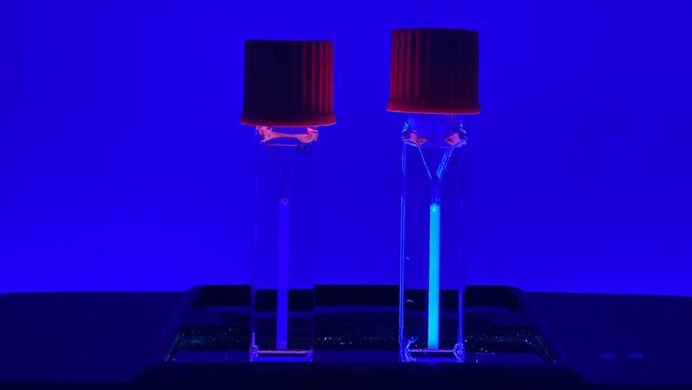
To enable the use of lower – and safer – ultrasound intensities, the researchers turned to gas vesicles (GVs), air-filled protein nanostructures that can be used as ultrasound contrast agents. They hypothesized that the GVs could function as acousto-mechanical transducers to focus the ultrasound energy: when exposed to FUS, the GVs undergo cavitation with the resulting energy activating the mechanophore.

PCs are no longer the massive beige boxes that sit on your desk taking up a massive amount of working real estate. Thanks to modernization and miniaturization, PCs can now fit into a tiny box.
How tiny?
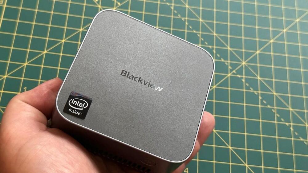
Well, a hockey puck is 3 inches in diameter and an inch thick, which is not a lot bigger than the Blackview MP80.
Need a powerful Windows 11 PC that’s not much bigger than a hockey puck and won’t cost you much? Then the Blackview MP80 is the mini PC for you.

Agriculture in Syria started with a bang 12,800 years ago as a fragmented comet slammed into the Earth’s atmosphere. The explosion and subsequent environmental changes forced hunter-gatherers in the prehistoric settlement of Abu Hureyra to adopt agricultural practices to boost their chances for survival.
That’s the assertion made by an international group of scientists in one of four related research papers, all appearing in the journal Science Open: Airbursts and Cratering Impacts. The papers are the latest results in the investigation of the Younger Dryas Impact Hypothesis, the idea that an anomalous cooling of the Earth almost 13 millennia ago was the result of a cosmic impact.
“In this general region, there was a change from more humid conditions that were forested and with diverse sources of food for hunter-gatherers, to drier, cooler conditions when they could no longer subsist only as hunter-gatherers,” said Earth scientist James Kennett, a professor emeritus of UC Santa Barbara. The settlement at Abu Hureyra is famous among archaeologists for its evidence of the earliest known transition from foraging to farming. “The villagers started to cultivate barley, wheat and legumes,” he noted. “This is what the evidence clearly shows.”


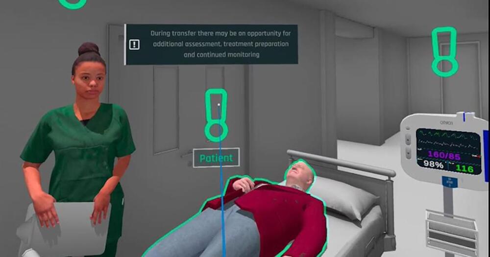
Annika Hauptvogel, head of technology and innovation management at Siemens, describes the industrial metaverse as “immersive, making users feel as if they’re in a real environment; collaborative in real time; open enough for different applications to seamlessly interact; and trusted by the individuals and businesses that participate”—far more than simply a digital world.
The industrial metaverse will revolutionize the way work is done, but it will also unlock significant new value for business and societies. By allowing businesses to model, prototype, and test dozens, hundreds, or millions of design iterations in real time and in an immersive, physics-based environment before committing physical and human resources to a project, industrial metaverse tools will usher in a new era of solving real-world problems digitally.
“The real world is very messy, noisy, and sometimes hard to really understand,” says Danny Lange, senior vice president of artificial intelligence at Unity Technologies, a leading platform for creating and growing real-time 3D content. “The idea of the industrial metaverse is to create a cleaner connection between the real world and the virtual world, because the virtual world is so much easier and cheaper to work with.”

Tap through to read how, for almost 30 years, a world-leading gait analysis laboratory at The Royal Children’s Hospital, Melbourne has helped children with cerebral palsy receive life-changing treatments → unimelb.me/45ez4RT
For almost 30 years, a world-leading gait analysis laboratory at The Royal Children’s Hospital in Melbourne has helped children with cerebral palsy receive life-changing treatments.
When Professor Kerr Graham arrived in Australia to introduce gait analysis technology to help manage children with cerebral palsy, some medical professionals were sceptical. An accomplished orthopaedic surgeon who had trained in Ireland, London and Toronto, Professor Graham had witnessed firsthand the dramatic potential of gait analysis to improve the lives of children with cerebral palsy.
However, in Australia, gait analysis was only being used by the Australian Institute of Sport in Canberra to help athletes perfect their performance. Professor Graham knew the technology had much to offer the approximate 2 in 1,000 Australian children born with cerebral palsy every year. He had seen it work and so, ignoring the sceptics, and with support from the Hugh Williamson Foundation and the Orthopaedic Department, he established Australia’s first clinical gait analysis laboratory at The Royal Children’s Hospital in Melbourne.