The engineering of structural deformations in light-sensitive semiconductors can boost the efficiency of solar cells.
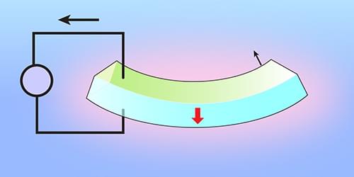
The quest for an efficient method to convert solar energy into electricity is crucial in the pursuit of carbon neutrality and environmental sustainability. Traditional solar cells are based on junctions between semiconductors, where a current is produced by photogenerated carriers separated by an electric field at the junction. Efforts to enhance solar-cell performance have focused on refining semiconductor properties and on perfecting devices. Concurrently, researchers are exploring alternative photovoltaic mechanisms that could work in synergy with the junction-based photovoltaic effect to boost solar-cell efficiency. Within this context, the engineering of a strain gradient in the material has emerged as a promising research direction. In this phenomenon, known as the flexophotovoltaic effect, an inhomogeneous strain in the material produces a photovoltaic effect in the absence of a junction [1].