Toggle light / dark theme

New strategy can directly pattern 2D materials into high-quality wafer-scale arrays

Two-dimensional (2D) semiconductors, materials that can conduct electricity and are only a few atoms thick, are promising alternatives to the conventional silicon-based semiconductors currently used to fabricate many electronics. Despite their promise, these materials have not yet been deployed on a large scale.

One reason for this is that reliably synthesizing them and patterning them to produce wafers (i.e., circular substrates employed in the manufacturing of electronics) has so far proved challenging. In fact, many existing patterning techniques rely on or polymer masks, both of which can leave unwanted residues on a wafer or damage the surface of 2D .

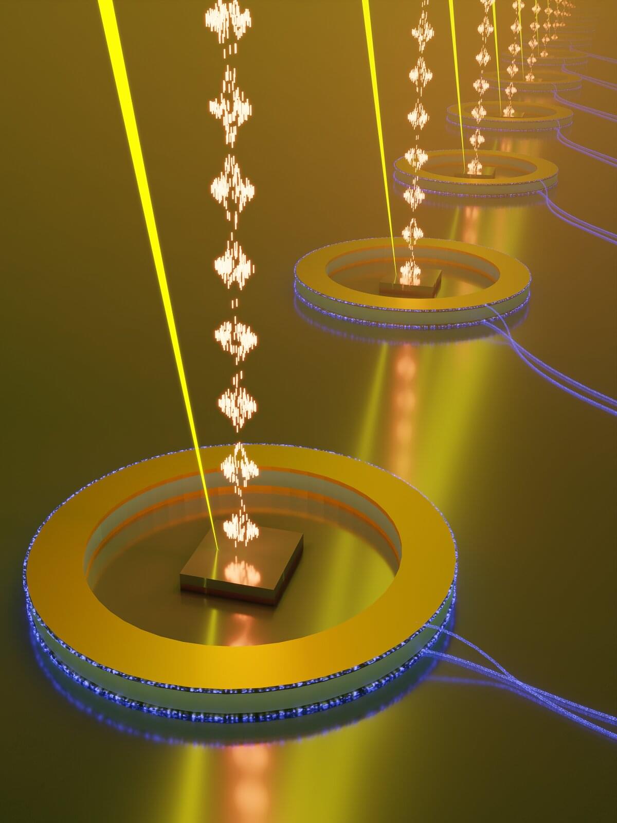
Researchers at Nanyang Technological University recently developed a new strategy to pattern 2D films into high-quality wafer-scale arrays, without damaging them or introducing undesirable residues. Their proposed method, outlined in a paper published in Nature Electronics, entails the use of a metal stamp producing three-dimensional (3D) patterns, which can be pressed onto 2D materials to produce a wafer with desired patterns.

Nanotechnology in AI: Building Faster, Smaller, and Smarter Systems

As artificial intelligence (AI) rapidly advances, the physical limitations of conventional semiconductor hardware have become increasingly apparent. AI models today demand vast computational resources, high-speed processing, and extreme energy efficiency—requirements that traditional silicon-based systems struggle to meet. However, nanotechnology is stepping in to reshape the future of AI by offering solutions that are faster, smaller, and smarter at the atomic scale.

The recent article published by AZoNano provides a compelling overview of how nanotechnology is revolutionizing the design and operation of AI systems, pushing beyond the constraints of Moore’s Law and Dennard scaling. Through breakthroughs in neuromorphic computing, advanced memory devices, spintronics, and thermal management, nanomaterials are enabling the next generation of intelligent systems.

Study outlines alternative approach to detecting inelastic dark matter particles

It is now understood that all known matter, i.e., studied by science and harnessed by technology, constitutes only 5% of the content of the universe. The rest is composed of two unknown components: dark matter (about 27%) and dark energy (about 68%). This calculation, confirmed decades ago, continues to surprise both lay people and scientists alike.

In the case of dark matter (DM), there is abundant evidence that it really exists, all resulting from its with ordinary matter. This evidence comes from sources such as the rotation curves of stars in galaxies, discrepancies in the movement of galaxies in clusters, the formation of large-scale structures in the universe, and cosmic background radiation, which is distributed uniformly throughout space.

Despite knowing with a high degree of certainty that DM exists, we do not know what it is. Several models proposed thus far have failed.

Simulations prove early Earth’s liquid core generated protective magnetic field

Earth is fortunate in having a magnetic field: it protects the planet and its life from harmful cosmic radiation. Other planets in our solar system—such as Mars—are constantly bombarded by charged particles that make life difficult.

Compact setup successfully detects elusive antineutrinos from nuclear reactor

Neutrinos are extremely elusive elementary particles. Day and night, 60 billion of them stream from the sun through every square centimeter of Earth every second, which is transparent to them. After the first theoretical prediction of their existence, decades passed before they were actually detected. These experiments are usually extremely large to account for the very weak interaction of neutrinos with matter.

Scientists at the Max Planck Institute for Nuclear Physics (MPIK) in Heidelberg have now succeeded in detecting antineutrinos from the reactor of a using the CONUS+ experiment, with a detector mass of just 3 kg. The work is published in Nature.

Originally based at the Brokdorf nuclear power plant, the CONUS experiment was relocated to the Leibstadt nuclear power plant (KKL) in Switzerland in the summer of 2023. Improvements to the 1 kg germanium semiconductor detectors, as well as the excellent measurement conditions at KKL, made it possible for the first time to measure what is known as Coherent Elastic Neutrino-Nucleus Scattering (CEvNS).

Building electronics that don’t die: Columbia’s breakthrough at CERN

Deep beneath the Swiss-French border, the Large Hadron Collider unleashes staggering amounts of energy and radiation—enough to fry most electronics. Enter a team of Columbia engineers, who built ultra-rugged, radiation-resistant chips that now play a pivotal role in capturing data from subatomic particle collisions. These custom-designed ADCs not only survive the hostile environment inside CERN but also help filter and digitize the most critical collision events, enabling physicists to study elusive phenomena like the Higgs boson.

SOSV bets plasma will change everything from semiconductors to spacecraft

It sees so much potential that it plans on investing in more than 25 plasma-related startups over the next five years. It is also opening a new Hax lab space in partnership with the New Jersey Economic Development Authority and the U.S. Department of Energy’s Princeton Plasma Physics Laboratory.

Nuclear fusion is an obvious place to seed plasma startups. The potential power source works by compressing fuel until it turns into a dense plasma, so dense that atoms begin fusing, releasing energy in the process.

“There’s so much here. The best ideas have yet to come to unlock a lot of potential in the fusion space,” Duncan Turner, general partner at SOSV, told TechCrunch.

Chemistry at the beginning: How molecular reactions influenced the formation of the first stars

Immediately after the Big Bang, which occurred around 13.8 billion years ago, the universe was dominated by unimaginably high temperatures and densities. However, after just a few seconds, it had cooled down enough for the first elements to form, primarily hydrogen and helium. These were still completely ionized at this point, as it took almost 380,000 years for the temperature in the universe to drop enough for neutral atoms to form through recombination with free electrons. This paved the way for the first chemical reactions.

The oldest molecule in existence is the helium hydride ion (HeH⁺), formed from a neutral helium atom and an ionized hydrogen nucleus. This marks the beginning of a chain reaction that leads to the formation of molecular hydrogen (H₂), which is by far the most common molecule in the universe.

Recombination was followed by the “dark age” of cosmology: although the universe was now transparent due to the binding of , there were still no light-emitting objects, such as stars. Several hundred million years passed before the first stars formed.

Light Versus Light: The Secret Physics Battle That Could Rewrite the Rules

In a fascinating dive into the strange world of quantum physics, scientists have shown that light can interact with itself in bizarre ways—creating ghost-like virtual particles that pop in and out of existence.

This “light-on-light scattering” isn’t just a theoretical curiosity; it could hold the key to solving long-standing mysteries in particle physics.

Quantum light: why lasers don’t clash like lightsabers.

/* */