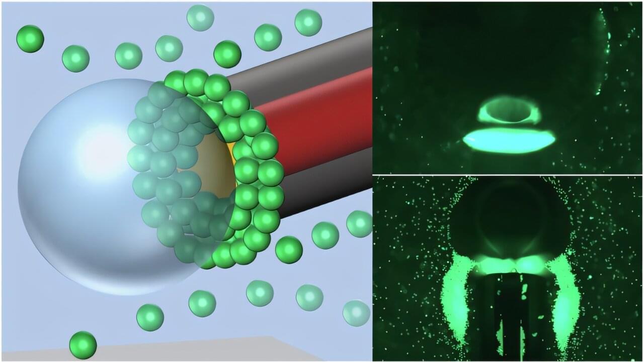
Menu

Blog

Archive for the ‘nanotechnology’ category: Page 8

Feb 28, 2024

Beyond Moore’s Law: New Strategy for Developing Highly Versatile Electronics With Outstanding Performance Discovered

Posted by in categories: computing, economics, nanotechnology

The miniaturization of electronic components, including transistors, has hit a plateau, presenting obstacles in the production of semiconductors. Nonetheless, a group of researchers, led by experts in materials science from the City University of Hong Kong (CityUHK), has unveiled a novel approach for creating highly versatile and high-performing electronics using transistors made of mixed-dimensional nanowires and nanoflakes. This breakthrough facilitates easier chip circuitry design and promotes the development of future electronic devices that are both flexible and energy-efficient.

In recent decades, as the continuous scaling of transistors and integrated circuits has started to reach physical and economic limits, fabricating semiconductor devices in a controllable and cost-effective manner has become challenging. Further scaling of transistor size increases current leakage and thus power dissipation. Complex wiring networks also have an adverse impact on power consumption.

Multivalued logic (MVL) has emerged as a promising technology for overcoming increasing power consumption. It transcends the limitations of conventional binary logic systems by greatly reducing the number of transistor components and their interconnections, enabling higher information density and lower power dissipation. Significant efforts have been devoted to constructing various multivalued logic devices, including anti-ambipolar transistors (AAT).

Feb 27, 2024

Researchers develop new nanoparticle to deliver drugs to immune system cells

Posted by in categories: biotech/medical, chemistry, engineering, nanotechnology

Vanderbilt researchers have developed a new nanoparticle that can more get drugs inside cells to boost the immune system and fight diseases such as cancer.

The research is led by John Wilson, associate professor of chemical and and , as well as a corresponding author on the paper about the research that was recently published in the journal Nanoscale.

Wilson, who is Principal Investigator of the Immunoengineering Lab at Vanderbilt and a Chancellor Faculty Fellow, and his team created a polymeric nanoparticle that can penetrate cell membranes and get drugs into the cytosol—or liquid—inside cells.

Feb 26, 2024

The 10 Stages of Artificial Intelligence

Posted by in categories: augmented reality, bioengineering, biological, genetics, nanotechnology, quantum physics, Ray Kurzweil, robotics/AI, singularity, transhumanism

https://www.youtube.com/watch?v=tFx_UNW9I1U&si=QxOgeE59dOkGDFck

This definitely is a Lifeboat post embodying what Lifeboat is about, and it’s only about AI. They did a really good job explaining the 10 stages.


This video explores the 10 stages of AI, including God-Like AI. Watch this next video about the Technological Singularity: • Technological Singularity: 15 Ways It…
🎁 5 Free ChatGPT Prompts To Become a Superhuman: https://bit.ly/3Oka9FM
🤖 AI for Business Leaders (Udacity Program): https://bit.ly/3Qjxkmu.
☕ My Patreon: / futurebusinesstech.
➡️ Official Discord Server: / discord.

Continue reading “The 10 Stages of Artificial Intelligence” »

Feb 26, 2024

Lab-spun sponges form perfect scaffolds for growing skin cells to heal wounds

Posted by in categories: biotech/medical, computing, engineering, nanotechnology

A new technique for electrospinning sponges has allowed scientists from the University of Surrey to directly produce 3D scaffolds—on which skin grafts could be grown from the patient’s own skin.

Electrospinning is a technique that electrifies droplets of liquid to form fibers from plastics. Previously, scientists had only been able to make 2D films. This is the first time anybody has electro-spun a 3D structure directly and on-demand so that it can be produced to scale. The research is published in the journal Nanomaterials.

Chloe Howard, from Surrey’s School of Computer Science and Electronic Engineering, said, After spinning these scaffolds, we grew skin cells on them. Seven days later, they were twice as viable as cells grown on 2D films or mats. They even did better than cells grown on plasma-treated polystyrene—previously, the gold standard. They were very happy cells on our 3D scaffolds.

Feb 25, 2024

Nanorobots in Clinical Practice: Advancing Towards Human Trials

Posted by in categories: biotech/medical, nanotechnology, robotics/AI

Discussions are emerging about conducting clinical trials on humans with nanorobots for medical applications. Currently, in the United States, four burgeoning companies are striving towards this aim, working to advance their nanomachines into Phase 1 studies, subsequent to laboratory research and preclinical trials on animals.

The article “Delivering drugs with microrobots”, published in Science on December 7, 2023, has recaptured the international scientific community’s attention on the practical, effective use of nanorobots in Clinical Practice and Medicine.

Its author, Bradley Nelson, a Robotics and Intelligent Systems professor at ETH Zurich, poses a straightforward question: where are these diminutive biocompatible machines, designed to be injected into the human body for more efficient exploration, internal repair, and precise, targeted drug delivery? Researchers have discussed them for years – he notes – yet we still do not see them progressing from laboratories to the forefront of clinical trials. How close are we to this milestone?

Feb 25, 2024

Research team develops nanoscale device for brain chemistry analysis

Posted by in categories: biotech/medical, chemistry, nanotechnology, neuroscience

Longstanding challenges in biomedical research such as monitoring brain chemistry and tracking the spread of drugs through the body require much smaller and more precise sensors. A new nanoscale sensor that can monitor areas 1,000 times smaller than current technology and can track subtle changes in the chemical content of biological tissue with sub-second resolution, greatly outperforming standard technologies.

The device, developed by researchers at the University of Illinois Urbana-Champaign, is silicon-based and takes advantage of techniques developed for microelectronics manufacturing. The small device size enables it to collect chemical content with close to 100% efficiency from highly localized regions of in a fraction of a second. The capabilities of this new nanodialysis device are reported in the journal ACS Nano.

“With our nanodialysis device, we take an established technique and push it into a new extreme, making problems that were impossible before quite feasible now,” said Yurii Vlasov, a U. of I. electrical & computer engineering professor and a co-lead of the study. “Moreover, since our devices are made on silicon using microelectronics fabrication techniques, they can be manufactured and deployed on large scales.”

Feb 24, 2024

Genetically engineered T cells for cancer immunotherapy

Posted by in categories: biotech/medical, chemistry, computing, genetics, nanotechnology

Relying on sub-wavelength nanostructures, metasurfaces have been shown as promising candidates for replacing conventional free-space optical components by arbitrarily manipulating the amplitude, phase, and polarization of optical wavefronts in certain applications1,2,3. In recent years, the scope of their applications has been expanded towards complete spatio-temporal control through the introduction of active metasurfaces. These developments open up exciting new possibilities for dynamic holography4, faster spatial light modulators5, and fast optical beam steering for LiDAR6. Large efforts have been channeled into various modulation mechanisms7. Microelectromechanical and nanoelectromechanical systems (MEMS and NEMS)8,9,10,11 have the advantages of low-cost and CMOS-compatibility, but the speed is limited up to MHz. Phase-change materials12,13,14 have fast, drastic, and non-volatile refractive index change, but lack continuous refractive index tuning and have a limited number of cycles constraining applicability to reconfigurable devices. Through molecule reorientation, liquid crystal can have index modulation over 10%, while under relatively low applied voltages Tunable liquid crystal metasurfaces, U.S. patent number 10,665,953 [Application Number 16/505,687]15. Techniques of liquid crystal integration have also advanced after decades of development. However, the tuning speeds are limited to kHz range16. Thermal-optic effects can induce relatively large refractive index changes17,18, but the speed is inherently limited and the on-chip thermal management can be challenging. The co-integration of transparent conductive oxide and metallic plasmonic structures5,6 has been demonstrated in epsilon-near-zero (ENZ) regime to control the wavefront of reflected light, but the low reflection amplitude induced by the optical loss of the materials and the ENZ regime is unavoidable.

In modern photonics, a multitude of technologies for tunable optics and frequency conversion19,20 are realized with nonlinear materials that have low loss and a strong χ effect, such as lithium niobate21,22, aluminum nitride23, and organic electro-optic (OEO) materials24. Their ultrafast responses make it possible to use RF or millimeter-wave control25. Developments in computational chemistry have also led to artificially engineered organic molecules that have record-high nonlinear coefficients with long-term and high-temperature stability26,27. However, their potential in modifying free-space light has been relatively unexplored until recently. Several OEO material-hybrid designs have demonstrated improved tunability of metasurfaces28,29,30. Utilizing dielectric resonant structures and RF-compatible coplanar waveguides, a free-space silicon-organic modulator has recently accomplished GHz modulation speed31. However, all demonstrations to date require high operating voltages ± 60V, due to low resonance tuning capability (frequency shift / voltage), which hinders their integration with electronic chips.

In this work, we propose combining high-Q metasurfaces based on slot-mode resonances with the unique nano-fabrication techniques enabled by OEO materials, which drastically reduces the operating voltage. The low voltage is mainly achieved from the ability to place the electrodes in close proximity to each other while hosting high-Q modes in between and the large overlap of the optical and RF fields in OEO materials. In the following sections, we first provide the design concepts and considerations for achieving a reduced operating voltage. Next, we numerically demonstrate the advantage of a particular selected mode compared to other supported modes in the structure. Finally, we experimentally realize our concepts and characterize the performance of the electro-optic metasurface.

Feb 23, 2024

Dynamic light manipulation via silicon-organic slot metasurfaces

Posted by in categories: chemistry, computing, nanotechnology

Relying on sub-wavelength nanostructures, metasurfaces have been shown as promising candidates for replacing conventional free-space optical components by arbitrarily manipulating the amplitude, phase, and polarization of optical wavefronts in certain applications1,2,3. In recent years, the scope of their applications has been expanded towards complete spatio-temporal control through the introduction of active metasurfaces. These developments open up exciting new possibilities for dynamic holography4, faster spatial light modulators5, and fast optical beam steering for LiDAR6. Large efforts have been channeled into various modulation mechanisms7. Microelectromechanical and nanoelectromechanical systems (MEMS and NEMS)8,9,10,11 have the advantages of low-cost and CMOS-compatibility, but the speed is limited up to MHz. Phase-change materials12,13,14 have fast, drastic, and non-volatile refractive index change, but lack continuous refractive index tuning and have a limited number of cycles constraining applicability to reconfigurable devices. Through molecule reorientation, liquid crystal can have index modulation over 10%, while under relatively low applied voltages Tunable liquid crystal metasurfaces, U.S. patent number 10,665,953 [Application Number 16/505,687]15. Techniques of liquid crystal integration have also advanced after decades of development. However, the tuning speeds are limited to kHz range16. Thermal-optic effects can induce relatively large refractive index changes17,18, but the speed is inherently limited and the on-chip thermal management can be challenging. The co-integration of transparent conductive oxide and metallic plasmonic structures5,6 has been demonstrated in epsilon-near-zero (ENZ) regime to control the wavefront of reflected light, but the low reflection amplitude induced by the optical loss of the materials and the ENZ regime is unavoidable.

In modern photonics, a multitude of technologies for tunable optics and frequency conversion19,20 are realized with nonlinear materials that have low loss and a strong χ effect, such as lithium niobate21,22, aluminum nitride23, and organic electro-optic (OEO) materials24. Their ultrafast responses make it possible to use RF or millimeter-wave control25. Developments in computational chemistry have also led to artificially engineered organic molecules that have record-high nonlinear coefficients with long-term and high-temperature stability26,27. However, their potential in modifying free-space light has been relatively unexplored until recently. Several OEO material-hybrid designs have demonstrated improved tunability of metasurfaces28,29,30. Utilizing dielectric resonant structures and RF-compatible coplanar waveguides, a free-space silicon-organic modulator has recently accomplished GHz modulation speed31. However, all demonstrations to date require high operating voltages ± 60V, due to low resonance tuning capability (frequency shift / voltage), which hinders their integration with electronic chips.

In this work, we propose combining high-Q metasurfaces based on slot-mode resonances with the unique nano-fabrication techniques enabled by OEO materials, which drastically reduces the operating voltage. The low voltage is mainly achieved from the ability to place the electrodes in close proximity to each other while hosting high-Q modes in between and the large overlap of the optical and RF fields in OEO materials. In the following sections, we first provide the design concepts and considerations for achieving a reduced operating voltage. Next, we numerically demonstrate the advantage of a particular selected mode compared to other supported modes in the structure. Finally, we experimentally realize our concepts and characterize the performance of the electro-optic metasurface.

Feb 23, 2024

Photon upconversion: Steering light with supercritical coupling

Posted by in categories: energy, nanotechnology, physics

National University of Singapore researchers and their collaborators have unveiled a novel concept termed “supercritical coupling” that enables a several-fold increase in photon upconversion efficiency. This discovery not only challenges existing paradigms, but also opens a new direction in the control of light emission.

Photon upconversion, the process of converting low-energy photons into higher-energy ones, is a crucial technique with broad applications, ranging from super-resolution imaging to advanced photonic devices. Despite considerable progress, the quest for efficient upconversion has faced challenges due to inherent limitations in the irradiance of lanthanide-doped nanoparticles and the critical coupling conditions of optical resonances.

The concept of “supercritical coupling” plays a pivotal role in addressing these challenges. This fundamentally new approach, proposed by a research team led by Professor Liu Xiaogang from the Department of Chemistry, NUS and his collaborator, Dr. Gianluigi Zito from the National Research Council of Italy leverages on the physics of “bound states in the continuum” (BICs).

Feb 23, 2024

“None of Us Expected This” — Scientists Have Discovered 2D Waveguides

Posted by in categories: nanotechnology, particle physics

The U.S. Naval Research Laboratory (NRL), working together with Kansas State University, has announced the discovery of slab waveguides made from the two-dimensional material hexagonal boron nitride. This milestone has been documented in the journal Advanced Materials.

Two-dimensional (2D) materials are a class of materials that can be reduced to the monolayer limit by mechanically peeling the layers apart. The weak interlayer attractions, or van der Waals attraction, allows the layers to be separated via the so-called “Scotch tape” method. The most famous 2D material, graphene, is a semimetallic material consisting of a single layer of carbon atoms. Recently, other 2D materials including semiconducting transition metal dichalcogenides (TMDs) and insulating hexagonal boron nitride (hBN) have also garnered attention. When reduced near the monolayer limit, 2D materials have unique nanoscale properties that are appealing for creating atomically thin electronic and optical devices.

Page 8 of 275First56789101112Last