Toggle light / dark theme

Not Science Fiction: Researchers Have Developed Metasurface Tractor Beams

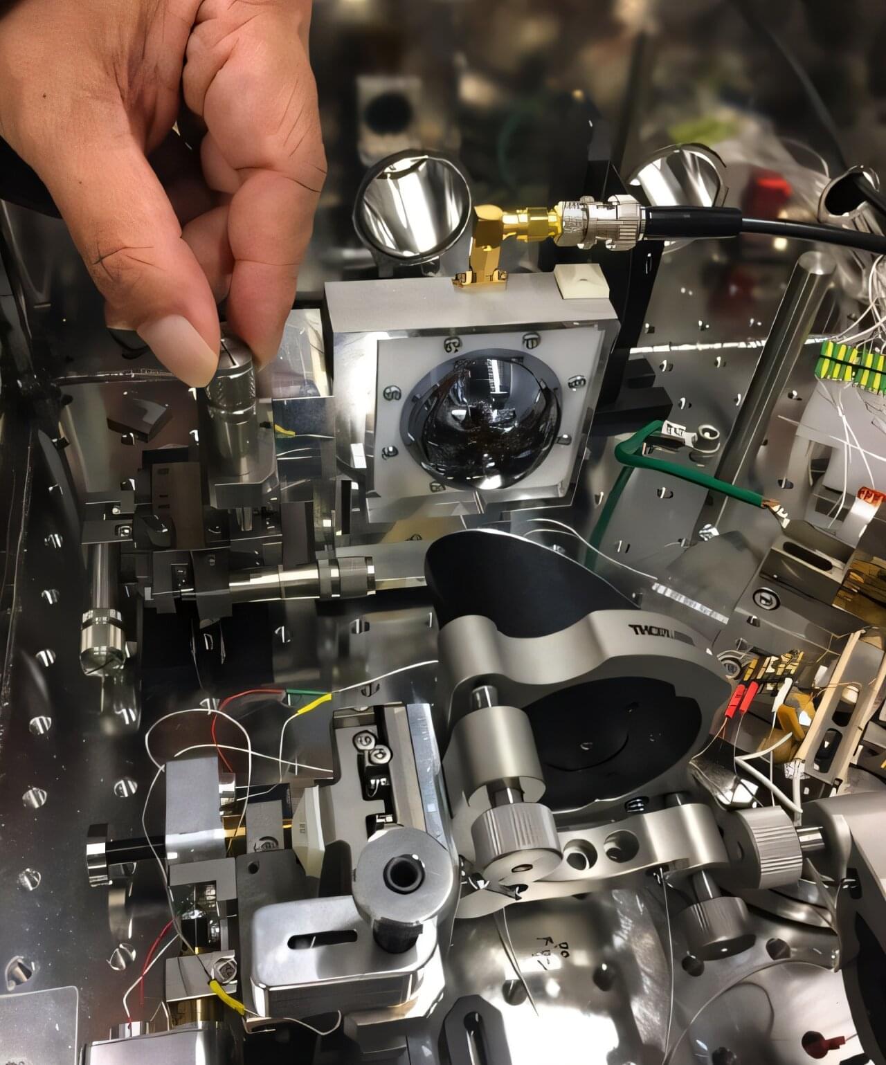
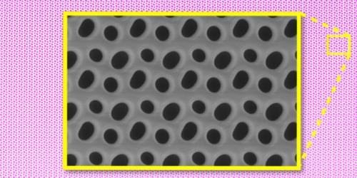
Researchers at TMOS have developed a metasurface-enabled solenoid beam that can pull particles towards it, potentially revolutionizing non-invasive medical procedures like biopsies. This technology, which uses a thin layer of nanopatterned silicon, offers a lightweight, portable alternative to the bulky equipment previously required for such beams. Credit: University of Melbourne.

Researchers at TMOS, the ARC Centre of Excellence for Transformative Meta-Optical Systems, have made a significant initial advancement in creating tractor beams enabled by metasurfaces. These beams of light, capable of drawing particles towards them, are inspired by the fictional tractor beams seen in science fiction.

In research published in ACS Photonics, the University of Melbourne team describes their solenoid beam that is generated using a silicon metasurface. Previous solenoid beams have been created by bulky special light modulators (SLMs), however, the size and weight of these systems prevent the beams from being used in handheld devices. The metasurface is a layer of nanopatterned silicon only about 1/2000 of a millimeter thick. The team hopes that one day it could be used to take biopsies in a non-invasive manner, unlike current methods such as forceps that cause trauma to the surrounding tissues.

Nano MIND: Scientists use magnetism to brain-control mice wirelessly

Unlocking the brain: how magnetic nanomaterials could transform neuroscience.

Mind-control magnet tech to regulate behavior, emotions, hunger.

Understanding the brain’s intricate networks and functions is a complex challenge.


Using magnetic fields and nanoparticles, researchers were able to increase and decrease feeding behavior and appetite in mice models.

Silicon Transformed: A Breakthrough in Laser Nanofabrication

A new method enables precise nanofabrication inside silicon using spatial light modulation and laser pulses, creating advanced nanostructures for potential use in electronics and photonics.

Silicon, the cornerstone of modern electronics, photovoltaics, and photonics, has traditionally been limited to surface-level nanofabrication due to the challenges posed by existing lithographic techniques. Available methods either fail to penetrate the wafer surface without causing alterations or are limited by the micron-scale resolution of laser lithography within Si.

In the spirit of Richard Feynman’s famous dictum, ‘There’s plenty of room at the bottom’, this breakthrough aligns with the vision of exploring and manipulating matter at the nanoscale. The innovative technique developed by the Bilkent team surpasses current limitations, enabling controlled fabrication of nanostructures buried deep inside silicon wafers with unprecedented control.

Integrating small-angle neutron scattering with machine learning enhances measurements of complex molecular structures

Small-angle scattering (SAS) is a powerful technique for studying nanoscale samples. So far, however, its use in research has been held back by its inability to operate without some prior knowledge of a sample’s chemical composition. Through new research published in The European Physical Journal E, Eugen Anitas at the Bogoliubov Laboratory of Theoretical Physics in Dubna, Russia, presents a more advanced approach, which integrates SAS with machine learning algorithms.

New method for determining the exchange energy of 2D materials

Ferromagnetism is an important physical phenomenon that plays a key role in many technologies. It is well-known that metals such as iron, cobalt and nickel are magnetic at room temperature because their electron spins are aligned in parallel — and it is only at very high temperatures that these materials lose their magnetic properties.

Researchers led by Professor Richard Warburton of the Department of Physics and the Swiss Nanoscience Institute of the University of Basel have shown that molybdenum disulfide also exhibits ferromagnetic properties under certain conditions. When subjected to low temperatures and an external magnetic field, the electron spins in this material all point in the same direction.

In their latest study, published in the journal Physical Review Letters (“Exchange energy of the ferromagnetic electronic ground state in a monolayer semiconductor”), the researchers determined how much energy it takes to flip an individual electron spin within this ferromagnetic state. This “exchange energy” is significant because it describes the stability of the ferromagnetism.