Boron, a chemical element next to carbon in the periodic table, is known for its unique ability to form complex bond networks. Unlike carbon, which typically bonds with two or three neighboring atoms, boron can share electrons among several atoms. This leads to a wide variety of nanostructures. These include boron fullerenes, which are hollow, cage-like molecules, and borophenes, ultra-thin metallic sheets of boron atoms arranged in triangular and hexagonal patterns.
Dr. Nevill Gonzalez Szwacki has developed a model explaining the variety of boron nanostructures. The analysis, published in the journal 2D Materials, combines more than a dozen known boron nanostructures, including the experimentally observed B₄₀ and B₈₀ fullerenes.
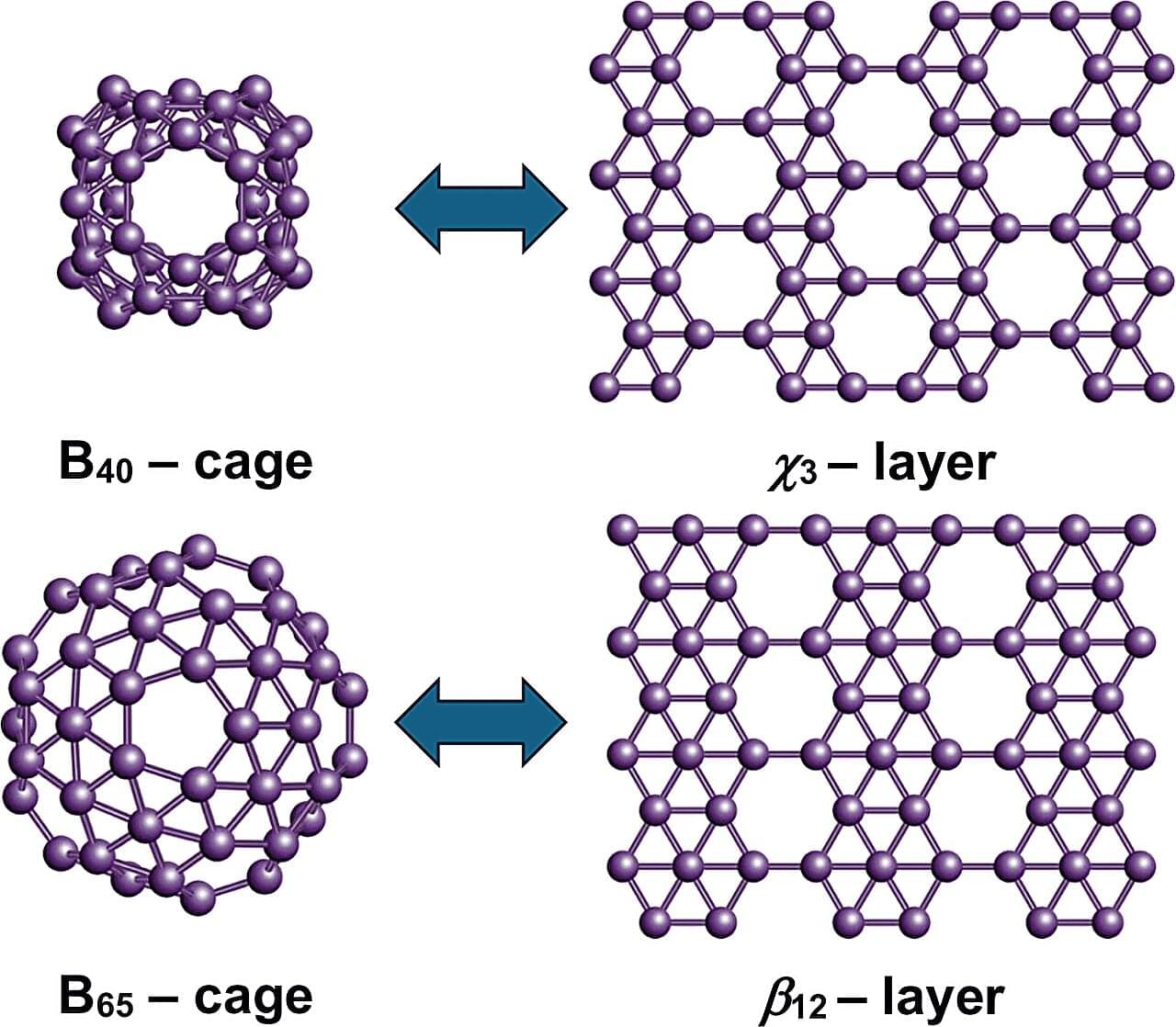
Using first-principles quantum-mechanical calculations, the study shows that the structural, energetic, and electronic properties of these systems can be predicted by looking at the proportions of atoms with four, five, or six bonds. The results reveal clear links between finite and extended boron structures. The B₄₀ cage corresponds to the χ₃ borophene layer, while B₆₅, B₈₀, and B₉₂ connect with the β₁₂, α, and bt borophene sheets, respectively. These structural links suggest that new boron cages could be created by using known two-dimensional boron templates.

