Toggle light / dark theme

Finding clarity in the noise: New approach recovers hidden signals at the nanoscale

In the world of nanotechnology, seeing clearly isn’t easy. It’s even harder when you’re trying to understand how a material’s properties relate to its structure at the nanoscale. Tools like piezoresponse force microscopy (PFM) help scientists peer into the nanoscale functionality of materials, revealing how they respond to electric fields. But those signals are often buried in noise, especially in instances where the most interesting physics happens.

Now, researchers at Georgia Tech have developed a powerful new method to extract meaningful information from even the noisiest data, or when, alternatively, the response of the material is the smallest. Their approach, which combines physical modeling with advanced statistical reconstruction, could significantly improve the accuracy and confidence of nanoscale measurement properties.

The team’s findings, led by Nazanin Bassiri-Gharb, Harris Saunders, Jr. Chair and Professor in the George W. Woodruff School of Mechanical Engineering and School of Materials Science and Engineering (MSE), are reported in Small Methods.

Quantum transport through a constriction in nanosheet gate-all-around transistors

In nanoscale transistors, quantum mechanical effects such as tunneling and quantization significantly influence device characteristics. However, large-scale quantum transport simulation remains a challenging field, making it difficult to account for quantum mechanical effects arising from the complex device geometries. Here, based on large-scale quantum transport simulations, we demonstrate that quantum geometrical effects in stacked nanosheet GAAFETs significantly impact carrier injection characteristics. Discontinuities in confinement energy at the constriction—the junction between the bulk source/drain and nanosheet channel—cause substantial carrier backscattering. This degradation becomes more severe as electrons experience higher effective energy barriers, and is further exacerbated at lower scattering rate, lower doping concentrations, and near Schottky barriers where electron depletion regions form. Considering these quantum mechanical bottlenecks, proper device optimization for future technology nodes requires a full quantum-based device structure design at the large-scale level, which enables unique optimization strategies beyond conventional classical prediction.


Kyoung Yeon Kim and colleagues report the importance of quantum geometrical effects that serve as a bottleneck in stacked nanosheet GAAFETs. This highlights that full quantum mechanics-based device design is crucial for realizing ideal carrier injection characteristics in future technology nodes.

Progress and Perspectives in 2D Piezoelectric Materials for Piezotronics and Piezo‐Phototronics

The emergence of two-dimensional (2D) materials has catalyzed significant advancements in the fields of piezotronics and piezo-phototronics, owing to their exceptional mechanical, electronic, and optical properties. This review provides a comprehensive examination of key 2D piezoelectric and piezo-phototronic materials, including transition metal dichalcogenides, hexagonal boron nitride (h-BN), and phosphorene, with an emphasis on their unique advantages and recent research progress. The underlying principles of piezotronics and piezo-phototronics in 2D materials is discussed, focusing on the fundamental mechanisms which enable these phenomena. Additionally, it is analyzed factors affecting piezoelectric and piezo-photoelectric properties, with a particular focus on the intrinsic piezoelectricity of 2D materials and the enhancement of out-of-plane polarization through various modulation techniques and materials engineering approaches. The potential applications of these materials are explored from piezoelectric nanogenerators to piezo-phototronic devices and healthcare. This review addresses future challenges and opportunities, highlighting the transformative impact of 2D materials on the development of next-generation electronic, optoelectronic, and biomedical devices.


This review examines advancements in 2D materials, focusing on their applications in piezotronics and piezo-phototronics. It discusses key materials like TMDs, h-BN, and phosphorene, highlighting their unique mechanical, electronic, and optical properties. The review delves into the mechanisms of piezoelectricity, explores applications such as nanogenerators and biomedical devices, and describes the future and challenges in 3D integration of 2D materials.

Room-Temperature Quantum Breakthrough Stuns Physicists

Scientists have achieved a breakthrough in quantum research by demonstrating that nanoparticles can exhibit quantum rotational vibrations even at room temperature — and without being cooled close to absolute zero. Using an elliptical nanoparticle held in an electromagnetic field, they applied car

Wave-like domain walls drive polarization switching in sliding ferroelectrics, study finds

Sliding ferroelectrics are a type of two-dimensional (2D) material realized by stacking nonpolar monolayers (atom-thick layers that lack an electric dipole). When these individual layers are stacked, they produce ferroelectric materials with an intrinsic polarization (i.e., in which positive and negative charges are spontaneously separated), which can be switched using an external electric field that is perpendicular to them.

Understanding the mechanisms driving the switching of this polarization in sliding ferroelectrics has been a key goal of many studies rooted in physics and materials science. This could ultimately inform the development of new advanced nanoscale electronics and quantum technologies.

Researchers at Westlake University and the University of Electronic Science and Technology of China recently uncovered a new mechanism that could drive the switching of polarization in sliding ferroelectrics. Their paper, published in Physical Review Letters (PRL), suggests that polarization switching in the materials is prompted by wave-like movements of domain walls (i.e., boundaries between regions with an opposite polarization), rather than by synchronized shifts affecting entire monolayers at once, as was assumed by some earlier works.

Wafer-scale nano-fabrication of multi-layer diffractive optical processors enables unidirectional visible imaging

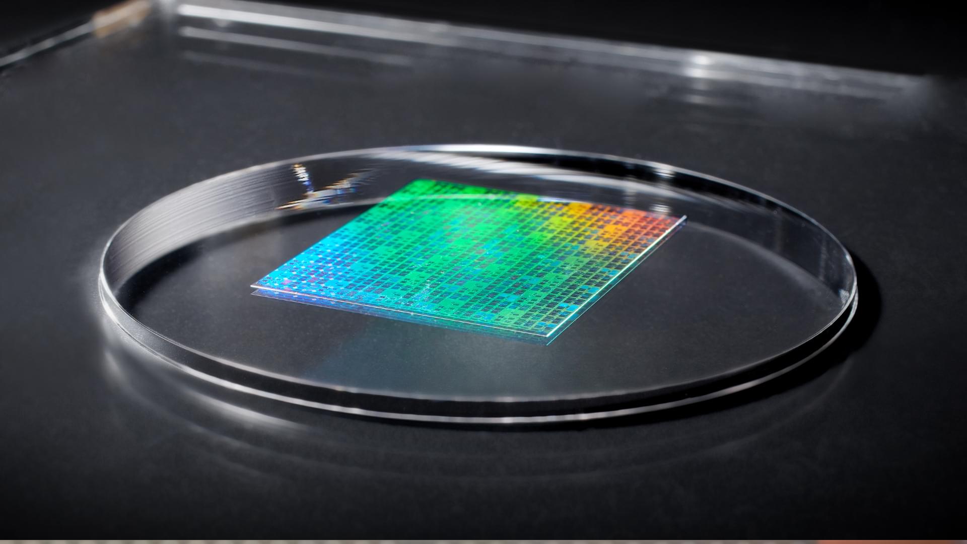
Researchers at the UCLA Samueli School of Engineering, in collaboration with the Optical Systems Division at Broadcom Inc., report a broadband, polarization-insensitive unidirectional imager that operates in the visible spectrum, capable of high-efficiency image transmission in one direction while effectively suppressing image formation in the reverse direction.

This device incorporates diffractive structures fabricated through wafer-scale lithography on high-purity fused silica, offering high optical transparency, and ultra-low loss.

The work appears in Light: Science & Applications.

Quantum dot technique improves multi-photon state generation

A photonics research group co-led by Gregor Weihs of the University of Innsbruck has developed a new technique for generating multi-photon states from quantum dots that overcomes the limitations of conventional approaches. This has immediate applications in secure quantum key distribution protocols, where it can enable simultaneous secure communication with different parties.

Quantum dots—semiconductor nanostructures that can emit on demand—are considered among the most promising sources for photonic quantum computing. However, every quantum dot is slightly different and may emit a slightly different color. This means that to produce multi-photon states, we cannot use multiple quantum dots.

Usually, researchers use a single quantum dot and multiplex the emission into different spatial and temporal modes, using a fast electro-optic modulator. The technological challenge is that faster electro-optic modulators are expensive and often require very customized engineering. To add to that, they may not be very efficient, which introduces unwanted losses into the system.

Surfaces, not confinement, rule until the thinnest limits

Researchers at the Max Planck Institute for Polymer Research have upended assumptions about how water behaves when squeezed into atom-scale spaces. By applying spectroscopic tools together with the machine learning simulation technique to water confined in a space of only a few molecules thick, the team, led by Mischa Bonn, found that water’s structure remains strikingly “normal” until confined to below a nanometer, far thinner than previously believed.

The research, “Interfaces Govern the Structure of Angstrom-Scale Confined Water Solutions,” was published in Nature Communications.

Peering into the structure of a layer of water molecules that is only a few molecules thick is a formidable scientific challenge. The team fabricated a nanoscale capillary device by trapping water between a single layer of graphene and a calcium fluoride (CaF₂) substrate. They then wielded cutting-edge vibrational surface-specific spectroscopy—capable of detecting the microscopic structure of confined water, including the orientation and hydrogen-bonding of water molecules—to “see” the elusive few layers of water.

Ultrathin metal and semiconductor films emit multicolor light, paving way for new optical sensing devices

A new breakthrough in the field of physics led by doctoral student Yueming Yan could allow for the creation of small, thin, low-power optical devices to be used in both medical imaging and environmental sensing.

In a study published in Science Advances, Yan and his colleagues, including Associate Professor of Chemistry Janet Macdonald and Stevenson Professor of Physics Richard Haglund, examined tiny nanoparticles of metals and semiconductors, specifically gold and copper.

The team laid down two ultrathin layers of gold and semiconducting copper sulfide nanoparticles, creating a “sandwich” 100 times thinner than a human hair. They then zapped this sandwich with a flash of light shorter than a trillionth of a second. Doing so caused the particles to “chat” back and forth, exchanging energy so efficiently that they re-emitted light in multiple different colors.

/* */