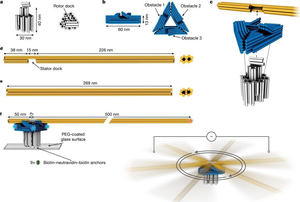
Motors are ubiquitous in our everyday lives — from cars to washing machines, even if we rarely notice them. A futuristic scientific field is working on the development tiny motors that could power a network of nanomachines and replace some of the power sources we currently use in electronic devices.
Researchers from the Cockrell School of Engineering at The University of Texas at Austin created the first ever solid-state optical nanomotor. All previous iterations of these light-driven motors reside in a solution of some sort, which limited their potential for the majority of real-world applications. This new research was published recently in the journal ACS Nano.
“Life started in the water and eventually moved on land,” said Yuebing Zheng, an associate professor in the Walker Department of Mechanical Engineering. “We’ve made these micro nanomotors that have always lived in solution work on land, in a solid state.”
