Menu

Blog

Archive for the ‘nanotechnology’ category: Page 133

May 14, 2022

The future of desalination? A fast, efficient, selective membrane for purifying saltwater

Posted by in categories: biotech/medical, computing, nanotechnology

Water scarcity is a growing problem around the world. Desalination of seawater is an established method to produce drinkable water but comes with huge energy costs. For the first time, researchers use fluorine-based nanostructures to successfully filter salt from water. Compared to current desalination methods, these fluorous nanochannels work faster, require less pressure and less energy, and are a more effective filter.

If you’ve ever cooked with a nonstick Teflon-coated frying pan, then you’ve probably seen the way that wet ingredients slide around it easily. This happens because the key component of Teflon is fluorine, a lightweight element that is naturally repelling, or hydrophobic. Teflon can also be used to line pipes to improve the flow of water. Such behavior caught the attention of Associate Professor Yoshimitsu Itoh from the Department of Chemistry and Biotechnology at the University of Tokyo and his team. It inspired them to explore how pipes or channels made from fluorine might operate on a very different scale, the nanoscale.

“We were curious to see how effective a fluorous nanochannel might be at selectively filtering different compounds, in particular, water and salt. And, after running some complex computer simulations, we decided it was worth the time and effort to create a working sample,” said Itoh. “There are two main ways to desalinate water currently: thermally, using heat to evaporate seawater so it condenses as pure water, or by , which uses pressure to force water through a that blocks salt. Both methods require a lot of energy, but our tests suggest fluorous nanochannels require little energy, and have other benefits too.”

May 14, 2022

J. Lyding & L. Grill | Silicon-Based Nanotechnology & Manipulating Single Molecules on Surfaces

Posted by in categories: biotech/medical, computing, nanotechnology, quantum physics

Foresight Molecular Machines Group.
Program & apply to join: https://foresight.org/molecular-machines/

Joe Lyding.
Silicon-Based Nanotechnology: There’s Still Plenty of Room at the Bottom.
Joe Lyding is a distinguished professor in Electrical and Computer Engineering at the University of Illinios. His career includes constructing the first atomic resolution scanning tunneling microscope, discovering new industrial uses for deuterium, studying quantum size effects down to 2nm lateral graphene dimensions, and much more. His current research is focused on carbon nanoelectronics. Specifically using carbon nanoelectronics based on carbon nanotubes and graphene for future semiconducting device applications.

Continue reading “J. Lyding & L. Grill | Silicon-Based Nanotechnology & Manipulating Single Molecules on Surfaces” »

May 13, 2022

Tailored single photons: Optical control of photons as the key to new technologies

Posted by in categories: nanotechnology, particle physics, quantum physics

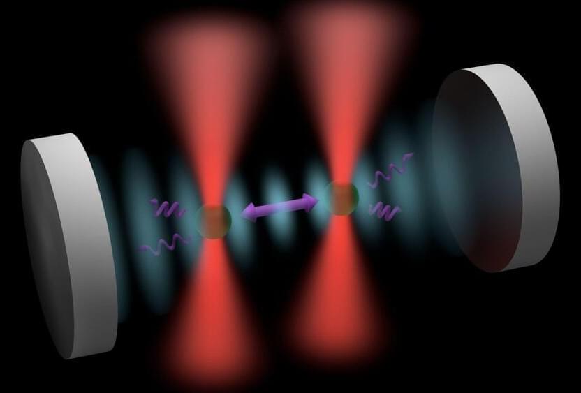
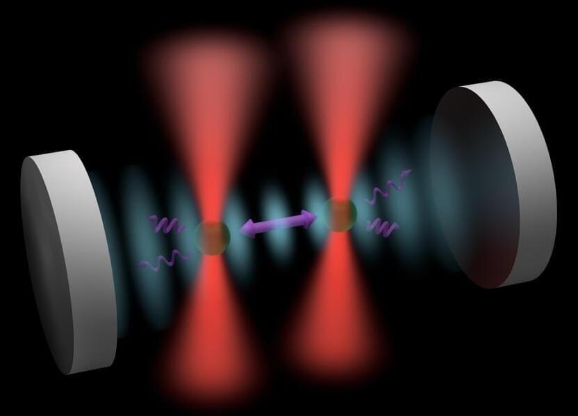
Physicists from Paderborn University have developed a novel concept for generating individual photons—tiny particles of light that make up electromagnetic radiation—with tailored properties, the controlled manipulation of which is of fundamental importance for photonic quantum technologies. The findings have now been published in the journal Nature Communications.

Professor Artur Zrenner, head of the “nanostructure optoelectronics” research group, explains how tailored desired states have so far posed a challenge: “Corresponding sources are usually based on light emissions from individual semiconductor quantum emitters, which generate the photons. Here, the properties of the emitted photons are defined by the fixed properties of the quantum emitter, and can therefore not be controlled with full flexibility.”

To get around the problem, the scientists have developed an all-optical, non-linear method to tailor and control single photon emissions. Based on this concept, they demonstrate laser-guided energy tuning and polarization control of photons (i.e., the light frequency and direction of oscillation of electromagnetic waves).

May 12, 2022

Scientists synthesize new, ultra-hard material

Posted by in categories: biotech/medical, engineering, military, nanotechnology

Russian scientists have synthesized a new ultra-hard material consisting of scandium containing carbon. It consists of polymerized fullerene molecules with scandium and carbon atoms inside. The work paves the way for future studies of fullerene-based ultra-hard materials, making them a potential candidate for photovoltaic and optical devices, elements of nanoelectronics and optoelectronics, and biomedical engineering as high-performance contrast agents. The study was published in Carbon.

The discovery of new, all-carbon molecules known as fullerenes almost 40 years ago was a revolutionary breakthrough that paved the way for fullerene nanotechnology. Fullerenes have a made of pentagons and hexagons that resembles a , and a cavity within the carbon frame of fullerene molecules can accommodate a variety of atoms.

The introduction of metal atoms into carbon cages leads to the formation of endohedral metallofullerenes (EMF), which are technologically and scientifically important owing to their unique structures and optoelectronic properties.

May 12, 2022

Quantum one-way street in topological insulator nanowires

Posted by in categories: computing, nanotechnology, quantum physics

Very thin wires made of a topological insulator could enable highly stable qubits, the building blocks of future quantum computers. Scientists see a new result in topological insulator devices as an important step towards realizing the technology’s potential.

An international group of scientists have demonstrated that wires more than 100 times thinner than a can act like a quantum one-way street for electrons when made of a peculiar material known as a .

The discovery opens the pathway for new technological applications of devices made from topological insulators and demonstrates a significant step on the road to achieving so-called topological qubits, which it has been predicted can robustly encode information for a quantum computer.

May 11, 2022

Cooling speeds up electrons in bacterial nanowires

Posted by in category: nanotechnology

The ground beneath our feet and under the ocean floor is an electrically-charged grid, the product of bacteria “exhaling” excess electrons through tiny nanowires in an environment lacking oxygen.

Yale University researchers have been studying ways to enhance this natural electrical conductivity within nanowires 1/100,000th width of a human hair by identifying the mechanism of electron flow.

Bacteria producing nanowires made up of cytochrome OmcS. (Image: Ella Maru Studio)

May 11, 2022

A new method for exploring the nano-world

Posted by in categories: biotech/medical, nanotechnology, particle physics, sustainability

Scientists at the Max Planck Institute for the Science of Light (MPL) and Max-Planck-Zentrum für Physik und Medizin (MPZPM) in Erlangen present a large step forward in the characterization of nanoparticles. They used a special microscopy method based on interfereometry to outperform existing instruments. One possible application of this technique may be to identify illnesses.

Nanoparticles are everywhere. They are in our body as , lipid vesicles, or viruses. They are in our drinking water in the form of impurities. They are in the air we breath as pollutants. At the same time, many drugs are based on the delivery of , including the vaccines we have recently been given. Keeping with the pandemics, quick tests used for the detection the SARS-Cov-2 are based on nanoparticles too. The red line, which we monitor day by day, contains myriads of gold nanoparticles coated with antibodies against proteins that report infection.

Technically, one calls something a nanoparticle when its size (diameter) is smaller than one micrometer. Objects of the order of one micrometer can still be measured in a normal microscope, but particles that are much smaller, say smaller than 0.2 micrometers, become exceedingly difficult to measure or characterize. Interestingly, this is also the size range of viruses, which can become as small as 0.02 micrometers.

May 11, 2022

A simpler approach for creating quantum materials

Posted by in categories: nanotechnology, quantum physics

Since graphene was first isolated and characterized in the early 2000s, researchers have been exploring ways to use this atomically thin nanomaterial because of its unique properties such as high tensile strength and conductivity.

In more recent years, twisted bilayer graphene, made of two sheets of graphene twisted to a specific “magic” angle, has been shown to have superconductivity, meaning that it can conduct electricity with very little resistance. However, using this approach to make devices remains challenging because of the low yield of fabricating twisted bilayer graphene.

Now, a new study shows how patterned, periodic deformations of a single layer of graphene transforms it into a material with previously seen in twisted graphene bilayers. This system also hosts additional unexpected and interesting conducting states at the boundary. Through a better understanding of how unique properties occur when single sheets of graphene are subjected to periodic strain, this work has the potential to create quantum devices such as orbital magnets and superconductors in the future. The study, published in Physical Review Letters, was conducted by graduate student Võ Tiến Phong and professor Eugene Mele in Penn’s Department of Physics & Astronomy in the School of Arts & Sciences.

May 11, 2022

Nature-inspired self-sensing materials could lead to new developments in engineering

Posted by in categories: engineering, health, nanotechnology

The cellular forms of natural materials are the inspiration behind a new lightweight, 3D printed smart architected material developed by an international team of engineers.

The team, led by engineers from the University of Glasgow, mixed a common form of industrial plastic with carbon nanotubes to create a material which is tougher, stronger and smarter than comparable conventional materials.

The nanotubes also allow the otherwise nonconductive plastic to carry an throughout its structure. When the structure is subjected to mechanical loads, its electrical resistance changes. This phenomenon, known as piezoresitivity, gives the material the ability to “sense” its structural health.

May 11, 2022

Design of effective self-powered SnS2/halide perovskite photo-detection system based on triboelectric nanogenerator

Posted by in categories: chemistry, health, internet, nanotechnology, robotics/AI, wearables

On account of the improvement the Internet of things (IoTs) and smart devices, our lives have been noticeably facilitated in the past few years. Machines and devices are becoming more ingenious with the help of artificial intelligence and various sensors1,2. So, integrated circuits are necessary to provide convenient and effectual communication3 Since the first report on TENG by Wang’s group in 20124, triboelectric systems have been recognized as a proper choice to harvest and convert the energy from the environment5,6. Photodetectors, as one of the most significant types of sensors that can precisely convert incident light into electrical signals have attracted increasing attention in recent years. Various applications including photo-sensors, spectral analysis7,8, environment monitoring9, communication devices10, imaging11, take advantage of narrow band or broad band photodetectors from ultraviolet to terahertz wavelenght. Literature reviews show that the heterojunction/heterostructure based on 2D/3D materials have been widely used in PD applications. In fact, to attain high performance of PDs based heterojunction, the built-in electrical field is needed to suppress the photogenerated recombination and stimulating collection12. Although, Si based PDs offer reliably high performance results, their complexity and expensive manufacturing process have limited their expansion and adoptability for industrial purposes13,14,15. Hence, most available PDs are designed based on external power supplies such as electrochemical batteries for signal production and processing, their design not only increases the sensor’s dimension and weight, but also creates limitations for sensor maintenances16 which is not proper in the IoTs. In 2014, ZH Lin et al. and Zheng et al. represented an investigation on the self-powered PD based on TENG system3,17, and since then, self-driven PDs have been extensively investigated2,5,9,18,19,20. These devices can find potential applications in health monitoring systems such as heart checking21 and health protection from some detrimental radiation such as high levels of UV radiance22.

But in the other hand, even though TENGs could be promise for using in wearable electronics, they still inevitably have limitations in power generation, sensing range, sensitivity, and also the sensing domain for the intrinsic limitations of electrification23,24,25. Moreover, due to high voltage, low current, and alternating current output of the TENGs, they cannot be used in order to supply power to electronic devices effectively without using power management circuits (PMCs) based on the LC modules. There are several reports that describe the importance of the impedance matching of the TENG and PMC units for better energy storage efficiency of the pulsed-TENG26,27. Without using the PMC unit, there are some challenges as a result of synching the TENG, as the power supply, and the consumption element such as the PD device. These challenges include the process of matching the resistance of the device and the impedance of the TENG to achieve effective performance of the self-powered system6,28.

In this study an efficient battery-free photodetector based on bulk heterojunction SnS2 nanosheets and perovskite materials has been designed and powered employing three different TENGs (GO paper/ Kapton, FTO/Kapton and hand/ FTO). In the first step for circuit designing to have better performance of the photodetector in coupling with TENG, the effect load resistance amount in the circuit on the impedance matching the TENG and the inner resistance of the photodetector, has been investigated through output current amplitude. The investigation, shows that to achieve the high amount of the photocurrent, the load resistance should be positioned in both critical zone of the out-put voltage of the TENG and the resistance range of high power density production of the TENG. In the second step, for investigation the effect of the dark resistance of the photodetector on out-put current of the self-powered photodetector, a device with very lower initial resistance (All-oxide Cu2O/ZnO photodetector) has been used with and without different load resistance in the circuit; in this regard, it is concluding that the initial resistance is too important to have proper design impedance matching circuit.