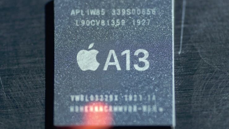
Apple’s A13 proceessor for the iPhone 11 lineup featurs 8.5 billion transistors and 20% performance improvements all around. Take a look!
Category: mobile phones – Page 137
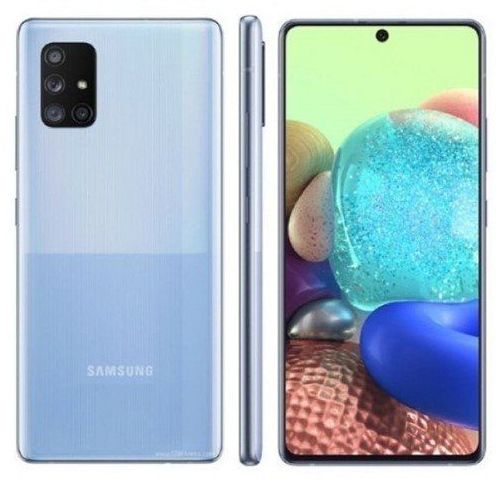
Samsung Galaxy A Quantum
Posted in mobile phones, security
The dimension of the smartphone is 162.5 × 75.5 × 8.1 mm and it weighs 185 grams. The smartphone has a Super AMOLED capacitive touchscreen providing 1080 × 2400 pixels resolution with 393 PPI density. The screen is also protected with Corning Gorilla Glass 3.
The rear camera of the smartphone consists of a 64 MP (wide) + 12 MP (ultrawide) + 5 MP (macro) + 5 MP (depth) while on the front there is a 32 MP (wide) camera for shooting selfies. The smartphone is available in various color options such as Prism Cube Black, Prism Cube Sliver, and Prism Cube Blue.
The Samsung Galaxy A Quantum is powered by the Exynos 980 (8 nm), QRNG security chipset Octa-core processor. The smartphone is fueled with a non-removable Li-Po 4500 mAh battery + Fast battery charging 25W.
TL;DR 206 | The Google Developer News Show
0:00 Android 11 Beta → https://goo.gle/3fzChBS
0:24 Introducing Google Play Asset Delivery → https://goo.gle/30R2pEn
0:47 Firebase Crashlytics SDK now publicly available → https://goo.gle/30SQxS8
1:05 Filestore now supports high performance → https://goo.gle/2YchJtr
1:33 New features from Google Maps Platform → https://goo.gle/3hCoRHd
1:53 Custom Cloud Monitoring dashboards → https://goo.gle/2AKHmsq
2:15 Introducing table-level access controls in BigQuery → https://goo.gle/3fzMcaJ
2:39 Introducing cross-region replica for Cloud SQL → https://goo.gle/2Bj9p1Q
2:49 Announcing sound null safety for Dart → https://goo.gle/2UTnEBr
Here to bring you the latest developer news from across Google is Developer Advocate Timothy Jordan. Tune in every week for a new episode, and let us know what you think of the latest announcements in the comments below! 😃
Follow Google Developers on Instagram → https://goo.gle/googledevs
Watch more #DevShow → https://goo.gle/GDevShow
The coronavirus has killed dozens of federal prisons and infected more than 6,000. Prisoners say they have been stuck in grim conditions that make social distancing impossible. To support their claims, some prisoners have used contraband cell phones that have been smuggled into prisons to post videos on Facebook and other social media sites.
VICE News contacted one of the prisoners, 34-year-old Aaron Campbell, held at a federal prison in Ohio, who said he was punished for making his video by being sent to solitary confinement. In a letter, Campbell said officials told him he would not face additional discipline if he issued a statement saying the video was fake. He refused. (The BOP did not respond to questions about his allegations.)
Read the full story — https://bit.ly/3dae6Zb
Check out VICE News for more: http://vicenews.com
In the last few years, most of the data such as books, videos, pictures, medical and even the genetic information of humans are moving toward digital formats. Laptops, tablets, smartphones and wearable devices are the major source of this digital data transformation and are becoming the core part of our daily life. As a result of this transformation, we are becoming the soft target of various types of cybercrimes. Digital forensic investigation provides the way to recover lost or purposefully deleted or hidden files from a suspect’s device. However, current man power and government resources are not enough to investigate the cybercrimes. Unfortunately, existing digital investigation procedures and practices require huge interaction with humans; as a result it slows down the process with the pace digital crimes are committed. Machine learning (ML) is the branch of science that has governs from the field of AI. This advance technology uses the explicit programming to depict the human-like behaviour. Machine learning combined with automation in digital investigation process at different stages of investigation has significant potential to aid digital investigators. This chapter aims at providing the research in machine learning-based digital forensic investigation, identifies the gaps, addresses the challenges and open issues in this field.
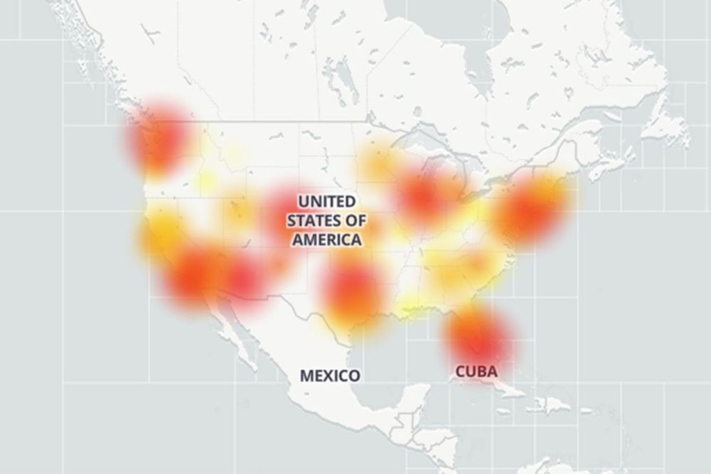
AMERICAN telecom customers experienced widespread cellphone outages during what was believed to be the largest cyberattack in US history.
Thousands of T-Mobile, Metro by T-Mobile, AT&T, Verizon, and Sprint customers all reported outages in areas including Florida, Georgia, New York, and California on Monday afternoon.
The disruptions were part of a large-scale distributed denial-of-service, or DDoS, attack meant to overwhelm an online service with multiple traffic sources to render it unusable, according to Pop Culture.
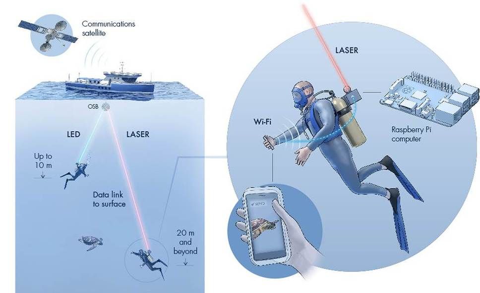
Radio waves travel poorly through the water, which makes it difficult for divers or submersibles to wirelessly transmit information to the surface. Scientists are trying to change that, though, by developing an underwater version of Wi-Fi.
Back in 2018, we heard how researchers at Saudi Arabia’s King Abdullah University of Science and Technology (KAUST) had used lasers to transmit HD video through water. Their experimental new system, known as Aqua-Fi, builds on that technology.
A user such as a scuba diver would start by sending data (such as photos or videos) from a smartphone contained in a watertight housing. That data would initially be transmitted in the form of radio waves, going just a few feet to a small device mounted on the diver’s air tanks.
Miniaturization has enabled technology like smartphones, health watches, medical probes and nano-satellites, all unthinkable a couple decades ago. Just imagine that in the course of 60 years, the transistor has shrunk from the size of your palm to 14 nanometers in dimension, 1000 times smaller than the diameter of a hair.
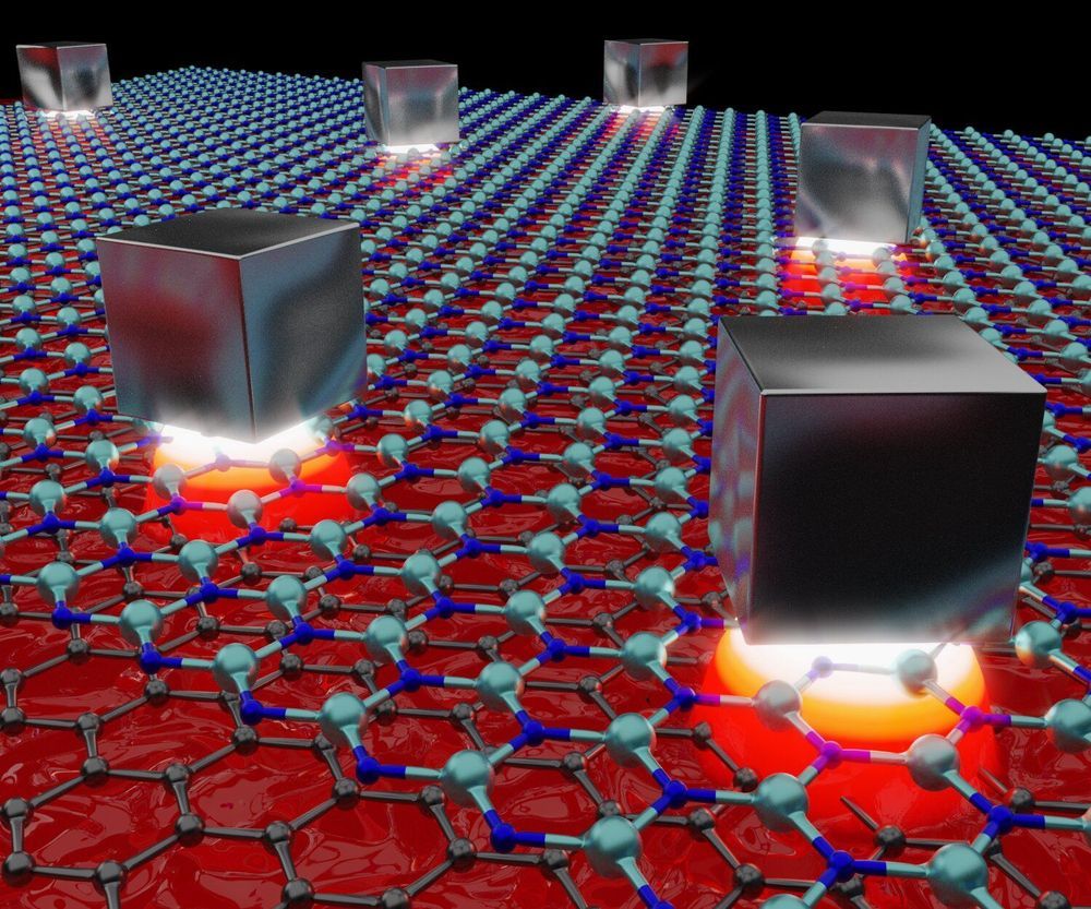
Miniaturization has pushed technology to a new era of optical circuitry. But in parallel, it has also triggered new challenges and obstacles, for example, controlling and guiding light at the nanometer scale. Researchers are looking for techniques to confine light into extremely tiny spaces, millions of times smaller than current ones. Studies had earlier found that metals can compress light below the wavelength-scale (diffraction limit).
In that aspect, graphene, a material composed from a single layer of carbon atoms, which exhibits exceptional optical and electrical properties, is capable of guiding light in the form of plasmons, which are oscillations of electrons that strongly interact with light. These graphene plasmons have a natural ability to confine light to very small spaces. However, until now, it was only possible to confine these plasmons in one direction, while the actual ability of light to interact with small particles like atoms and molecules resides in the volume into which it can be compressed. This type of confinement in all three dimensions is commonly regarded as an optical cavity.
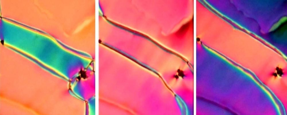
Researchers at the University of Colorado Boulder’s Soft Materials Research Center (SMRC) have discovered an elusive phase of matter, first proposed more than 100 years ago and sought after ever since.
The team describes the discovery of what scientists call a “ferroelectric nematic” phase of liquid crystal in a study published today in the Proceedings of the National Academy of Sciences. The discovery opens a door to a new universe of materials, said co-author Matt Glaser, a professor in the Department of Physics.
Nematic liquid crystals have been a hot topic in materials research since the 1970s. These materials exhibit a curious mix of fluid- and solid-like behaviors, which allow them to control light. Engineers have used them extensively to make the liquid crystal displays (LCDs) in many laptops, TVs and cellphones.
Mobile phones and computers are currently responsible for up to 8% of the electricity use in the world. This figure has been doubling each past decade but nothing prevents it from skyrocketing in the future. Unless we find a way for boosting energy efficiency in information and communications technology, that is. An international team of researchers, including Ikerbasque Research Associate Alexey Nikitin (DIPC), has just published in Nature 1 a breakthrough in quantum physics that could deliver exactly that: electronics and communications technology with ultralow energy consumption.
Future information and communication technologies will rely on the manipulation of not only electrons but also of light at the nanometer-scale. Squeezing light to such a small size has been a major goal in nanophotonics for many years. Particularly strong light squeezing can be achieved with polaritons, quasiparticles resulting from the strong coupling of photons with a dipole-carrying excitation, at infrared frequencies in two-dimensional materials, such as graphene and hexagonal boron nitride. Polaritons can be found in materials consisting of two-dimensional layers bound by weak van der Waals forces, the so-called van der Waals materials. These polaritons can be tuned by electric fields or by adjusting the material thickness, leading to applications including nanolasers, tunable infrared and terahertz detectors, and molecular sensors.
But there is a major problem: even though polaritons can have long lifetimes, they have always been found to propagate along all directions (isotropic) of the material surface, thereby losing energy quite fast, which limits their application potential.
