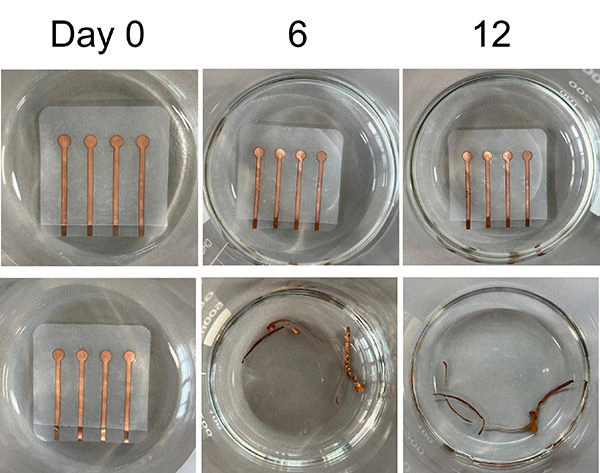
Many plastic products are designed to be used only once, yet the material itself lasts for years. But a new strategy is addressing this problem by creating products that self-destruct on command, known as living plastics. These materials incorporate activatable, plastic-degrading microbes alongside the polymers. One team reporting in ACS Applied Polymer Materials used two bacterial strains that worked together and completely broke down the material within just six days, without making microplastics.
Why scientists are rethinking plastics Zhuojun Dai, a corresponding author on the paper, explains that “the realization that traditional plastics persist for centuries, while many applications, like packaging, are short-lived, led us to ask: Could we build degradation directly into the material’s life cycle?”
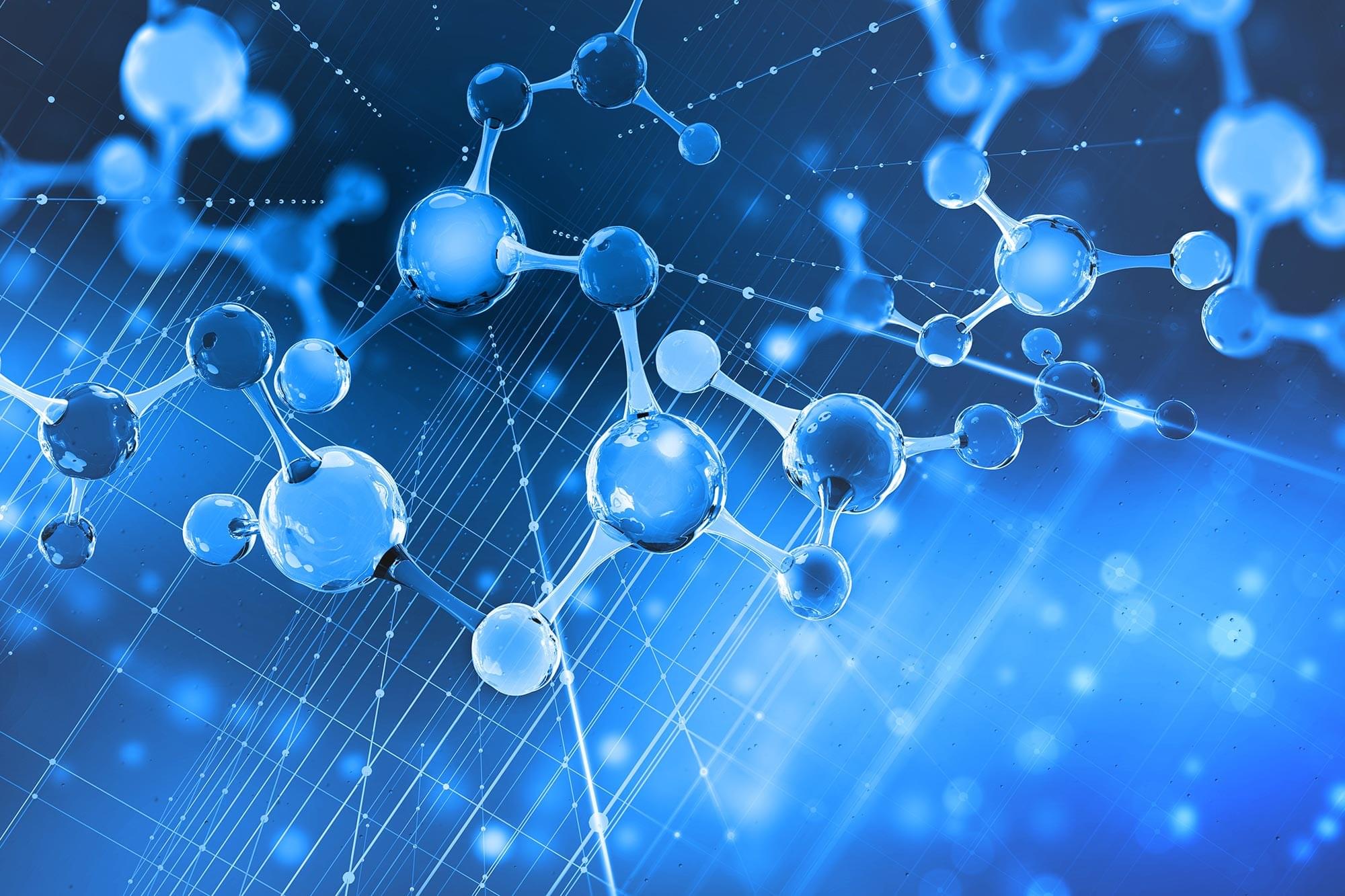
Many microbes can break long polymeric chains into smaller pieces using enzymes. Because plastics are polymers, these enzymes or the microbes that make them could be incorporated into living plastics.
 decay, particularly from tritium: Because the neutrino carries away part of the decay energy, a nonzero neutrino mass slightly modifies the spectrum of emitted electrons. Precision experiments such as KATRIN have pushed this method to its limit, setting an upper bound of about 0.45 eV on the neutrino mass [1]. While KATRIN uses molecular tritium gas, new strategies aim to go further by embedding tritium in engineered materials.