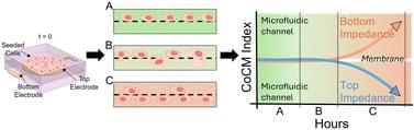
A new laboratory technique for measuring how quickly cells penetrate and pass through a porous membrane and reach the opposite side could help identify cancer cells with the greatest potential to spread in the human body.
The method relies on tiny electrodes placed on either side of an artificial membrane. The electrodes measure changes in electrical resistance as cells pass through the material. The most aggressive cancer cells pass through the membrane more rapidly than other cells.
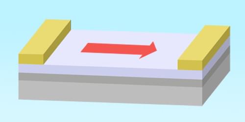
The illustration depicts cells (green and blue) moving through a membrane (grey) studded with microelectrodes (gold rings).
🔗
We present a novel microfluidic device capable of electrically interrogating both surfaces of a porous membrane quantitatively and in real time using electrical impedance spectroscopy to monitor cell migration. This device holds patterned gold electrodes on both sides of the membrane, which enable independent impedance measurements on each side of the membrane. We introduce the term cross-over cell migration (CoCM) to describe this dual-sided approach, which allows precise monitoring of cells at their seeding location and as they move through a porous membrane. To ensure reliable tracking, we developed a normalization method, the CoCM index, that allows us to compare both membrane surfaces directly in real-time. Human renal carcinoma cells (786-O) were passively seeded in the device’s top microfluidic chamber, and we collected impedance data from both sides of the membrane surfaces simultaneously over a three-day period. These measurements successfully captured the onset and progression of cell migration across the membrane interface. We tracked the cells with fluorescence imaging in parallel to validate our impedance data. As cells appeared in focus on the bottom-side electrode surface, their numbers kept increasing over the course of our experiment. The CoCM index decreased by about 20% in the top chamber and increased by approximately 15% in the bottom chamber. Symmetrical CoCM index trends appeared after 40 h, consistent with the fluorescent images captured. Finally, we performed live-cell fluorescence assays to confirm post-experiment cell viability and to quantify migrated cells, further validating our CoCM platform measurements. This platform is a valuable tool not only for real-time and quantitative cell migration studies of cancer and other cells in bulk but also for future studies of single-cell migration processes.