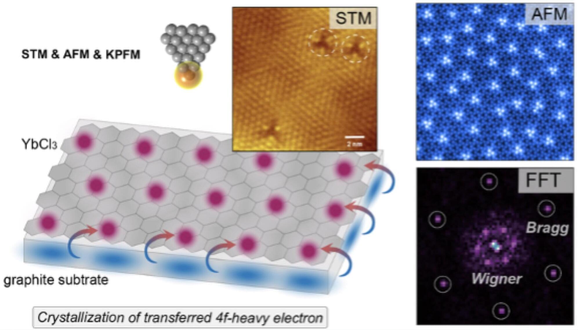
Toggle light / dark theme

Defect Characterization and Control in 2D Materials and Devices

As soon as 2DMs are employed for devices, at some point they have to be grown or transferred onto insulators. A wide range of insulators has already been suggested for the use with 2DMs, starting with the amorphous 3D oxides known from Si technologies (SiO2, HfO2, Al2O3), and expanding to native 2D oxides (MoO3, WO3, Bi2SeO5), layered 2D crystals (hBN, mica) and 3D crystals like fluorides (CaF2, SrF2, MgF2) or perovskites (SrTiO3, BaTiO3). These insulators also contain various defects which can also be detrimental to device stability and reliability. Again, on the other hand, these defects can be exploited for added functionality like resistive switching devices, neuromorphic devices, and sensors.

Finally, 2DMs need to be contacted with metals, which typically introduces defects in the 2DMs which then have a strong impact on the behaviour of the resulting Schottky contacts as they tend to pin the Fermi-level and result in large series resistances.

This collection aims to provide a comprehensive overview of the latest research on defect characterization and control in 2D materials and devices. By bringing together studies that utilize advanced theoretical calculations, such as density functional theory (DFT) and first-principles calculations, as well as experimental techniques like transmission electron microscopy (TEM), scanning tunneling microscopy (STM), X-ray photoemission spectroscopy (XPS), atomic force microscopy (AFM), and various optical spectroscopies, this collection seeks to deepen our understanding of defect formation, propagation, control, and their impact on device performance.

Molecular Decrowding by Tissue Expansion Allows Precise Determination of the Spatial Distribution of Synaptic Proteins at a Nanometer Scale by exTEM

To understand how the molecular machinery of synapses works, it is essential to determine an inventory of synaptic proteins at a subsynaptic resolution. Nevertheless, synaptic proteins are difficult to localize because of the low expression levels and limited access to immunostaining epitopes. Here, we report on the exTEM (epitope-exposed by expansion-transmission electron microscopy) method that enables the imaging of synaptic proteins in situ. This method combines TEM with nanoscale resolution and expandable tissue-hydrogel hybrids for enhanced immunolabeling with better epitope accessibility via molecular decrowding, allowing successful probing of the distribution of various synapse-organizing proteins. We propose that exTEM can be employed for studying the mechanisms underlying the regulation of synaptic architecture and function by providing nanoscale molecular distribution of synaptic proteins in situ. We also envision that exTEM is widely applicable for investigating protein nanostructures located in densely packed environments by immunostaining of commercially available antibodies at nanometer resolution.

Spin currents control device magnetization using low-cost materials

Research from the University of Minnesota Twin Cities gives new insight into a material that could make computer memory faster and more energy-efficient.

The study was recently published in Advanced Materials, a peer-reviewed scientific journal. The researchers also have a patent on the technology.

As technology continues to grow, so does the demand for emerging memory technology. Researchers are looking for alternatives and complements to existing memory solutions that can perform at high levels with low energy consumption to increase the functionality of everyday technology.

Iron oxide behavior under pressure may reduce reliance on rare-earth metals in consumer, energy and medical tech

Researchers at The University of Texas at Arlington have discovered a surprising new type of magnetic property that could lead to stronger magnets made from tiny particles of common iron oxide. This finding could enhance the performance of everyday technologies while reducing the need for rare-earth metals—materials that are more costly, less sustainable and harder to obtain.

New microscopy technique achieves 1-nanometer resolution for atomic-scale imaging

Understanding the interaction between light and matter at the smallest scales (angstrom scale) is essential for advancing technology and materials science. Atomic-scale structures, such as defects in diamonds or molecules in electronic devices, can significantly influence a material’s optical properties and functionality. To explore these tiny structures, we need to extend the capabilities of optical microscopy.

Researchers at the Fritz-Haber Institute of the Max-Planck Society, Germany, and their international collaborators at Institute for Molecular Science/SOKENDAI, Japan and CIC nanoGUNE, Spain have developed an approach to scattering-type scanning near-field optical microscopy (s-SNOM) that achieves a spatial resolution of 1 nanometer. This technique, termed as ultralow tip oscillation amplitude s-SNOM (ULA-SNOM), combines advanced microscopy methods to visualize materials at the atomic level.

The work is published in the journal Science Advances.

JWST finds unusual black hole in the center of the Infinity Galaxy: ‘How can we make sense of this?’

The researchers behind these findings uncovered the Infinity Galaxy while examining images from the JWST’s 255-hour treasury COSMOS-Web survey. In addition to the suspected direct collapse black hole that sits between the colliding galaxies, the team found that each nucleus of those galaxies also contains a supermassive black hole!

“Everything is unusual about this galaxy. Not only does it look very strange, but it also has this supermassive black hole that’s pulling a lot of material in,” team leader and Yale University researcher Pieter van Dokkum said in a statement. “The biggest surprise of all was that the black hole was not located inside either of the two nuclei but in the middle.

We asked ourselves: How can we make sense of this?

/* */