Microplastics are a growing environmental problem, but now researchers in Korea have developed a new water purification system that can filter out these tiny fragments, as well as other pollutants, very quickly and with high efficiency.
Given the ubiquity of plastic in the modern world, it’s not surprising that tiny flakes of the stuff can be found basically everywhere on Earth, even in environments thought to be pristine. Microplastics have been detected from pole to pole, from the deepest ocean trenches to the tallest mountain peaks, and are making their way up the food chain all the way to humans.
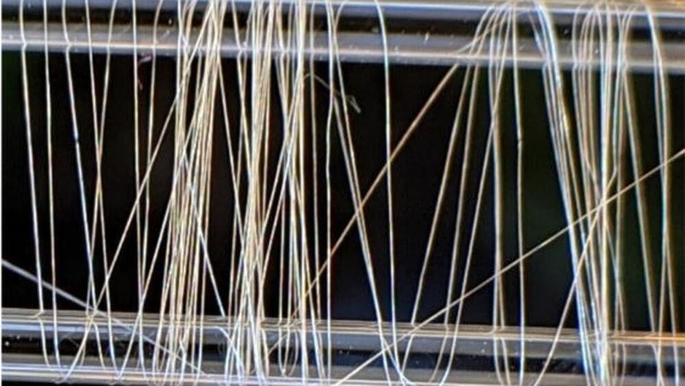
Various materials are being tested to help filter out microplastics, including magnetic “nanopillars,” nanocellulose, semiconductor wires, and filtration columns containing sand, gravel and biofilms. Now, researchers at Daegu Gyeongbuk Institute of Science and Technology (DGIST) in South Korea have found promise with a new design.