Another part of that wariness arises because, to date, no one has independently reproduced Dias’ team’s results. This lack of verification was raised by Jorge Hirsch of the University of California, San Diego, in the last talk of the session in which Dias and his team spoke. Hirsch argued that those claiming to have created high-temperature superconducting hydrides suffered from “confirmation bias,” cherry-picking evidence to support their agenda. (Hirsch has been an outspoken critic of Dias’ work.) As the last question of the session, Dias asked Hirsch, “Could you also have confirmation bias?” “Maybe,” Hirsch replied.
After the session, a few attending researchers—all collaborators of Dias—spoke with Physics Magazine, telling us that they disagreed with Hirsch’s cherry-picking conclusion. One of them, Russell Hemley of the University of Illinois Chicago confirmed Pasan’s claim that they have replicated the 2020 carbonaceous sulfur hydride—as reported in an arXiv paper that the team recently posted [3].
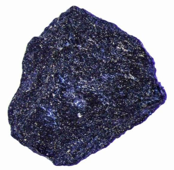
Dias’ group still needs to more precisely characterize NLH’s chemical composition, Pasan said. The samples also appear to consist of two phases, an observation that they need to investigate. Ultimately, they plan to innovate upon this material to create a superconductor at ambient pressure and temperature conditions, a goal that Pasan said he thinks is feasible. But extraordinary claims require extraordinary evidence, and the community has much of the latter still to gather.


