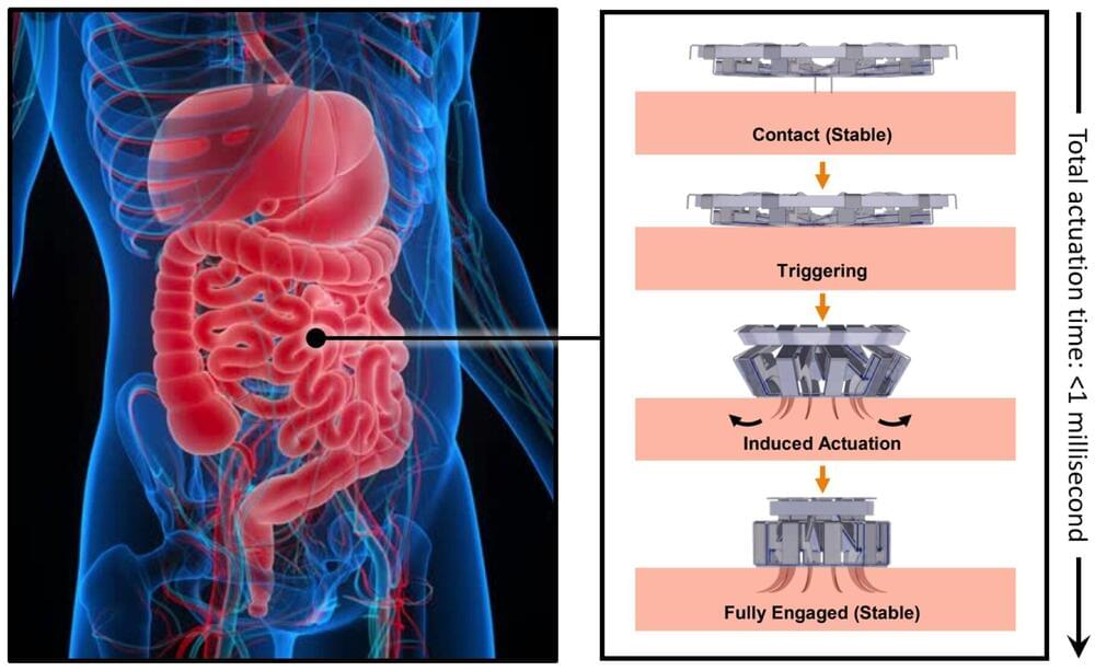
A growing number of firms are turning fungi roots into clothing and building material.
Category: materials – Page 118
Researchers at Kyushu University, the National Institute of Advanced Industrial Science and Technology (AIST) and Osaka University in Japan have recently introduced a new strategy for synthesizing multi-layer hexagonal boron nitride (hBN), a material that could be used to integrate different 2D materials in electronic devices, while preserving their unique properties. Their proposed approach, outlined in a paper published in Nature Electronics, could facilitate the fabrication of new highly performing graphene-based devices.
“The atomically flat 2D insulator hBN is a key material for the integration of 2D materials into electronic devices,” Hiroki Ago, one of the researchers who carried out the study, told Tech Xplore. “For example, the highest carrier mobility in monolayer graphene is achieved only when it is sandwiched by multilayer hBN. Superconductivity observed in twisted bilayer graphene also needs multilayer hBN to isolate from environment.”
In addition to its value for fabricating graphene-based devices, hBN can also be used to integrate transition metal dichalcogenides (TMDs) in devices, achieving strong photoluminescence and high carrier mobility. It can also be valuable for conducting studies focusing on moiré physics.
MANUFACTURA’s eggshell project transforms organic waste into a sustainable building material made from 3D printed eggshells.
Researchers from Southwest University in China have constructed the entire chromosomal-scale genome assembly and complete spidroin gene set of the golden orb-weaving spider, Trichonephila clavata, known for its especially strong, golden-colored webs.
They attest that their work “Provides multidimensional data that significantly expand the knowledge of spider dragline silk generation…” and the researchers plan on using this new “molecular atlas” to better understand how spiders manufacture their silk.
Published in the journal Nature Communications, the paper details the steps the researchers took, from wild spider capture to multiomic analysis, in revealing the interplay of genes within the spider’s major ampullate gland, the gland responsible for producing dragline silk.
A new RMIT-led international collaboration published in February has uncovered, for the first time, a distinct disorder-driven bosonic superconductor-insulator transition.
The discovery outlines a global picture of the giant anomalous Hall effect and reveals its correlation with the unconventional charge density wave in the AV3Sb5 kagome metal family, with potential applications in future ultra-low energy electronics.
Superconductors, which can transmit electricity without energy dissipation, hold great promise for the development of future low-energy electronics technologies, and are already applied in diverse fields such as hover trains and high-strength magnets (such as medical MRIs).
After testing several different types of grass and other raw materials, Plantd settled on a perennial (meaning it grows back every year and doesn’t need to be re-planted) long grass that can grow 20 to 30 feet in a year.
Though grass is obviously softer than wood, it contains a similar cellulose fiber that can be broken down then reconstituted and engineered in such a way that the final product is even stronger than wood (check out this video that made the rounds on LinkedIn last year: a regular wood panel and a Plantd panel are subjected to a sledgehammer, and just one of the two withstands the test).
Plantd makes structural building panels for wall sheathing, roof decking, and subflooring, and they say their product outcompetes wood on every metric: it’s stronger, cheaper, lighter, more moisture-resistant, and captures more carbon—all for the same cost as wood. The panels are meant to be a replacement for a plywood-like material called traditional oriented strand board, or OSB. Custom-built machinery uses heat and pressure to press shredded grass into panels, with a standard four-by-eight-foot panel using about 50 pounds of grass.
Imagine a sheet of material just one layer of atoms thick—less than a millionth of a millimeter. While this may sound fantastical, such a material exists: it is called graphene and it is made from carbon atoms in a honeycomb arrangement. First synthesized in 2004 and then soon hailed as a substance with wondrous characteristics, scientists are still working on understanding it.
Postdoc Areg Ghazaryan and Professor Maksym Serbyn at the Institute of Science and Technology Austria (ISTA) together with colleagues Dr. Tobias Holder and Professor Erez Berg from the Weizmann Institute of Science in Israel have been studying graphene for years and have now published their newest findings on its superconducting properties in a research paper in the journal Physical Review B.
“Multilayered graphene has many promising qualities ranging from widely tunable band structure and special optical properties to new forms of superconductivity—meaning being able to conduct electrical current without resistance,” Ghazaryan explains.
A team of scientists, including physicist Eugene Demler from ETH Zurich, for the first time, closely observed how magnetic correlations play a role in mediating hole pairing.
Superconductivity only occurs in pairs. Therefore, in order for conductance without electrical resistance to take place in specific materials, the charge carriers must pair up. In traditional superconductors, the current is made up of electrons and pairing is facilitated by the collective movements of the crystal lattice, referred to as phonons. This mechanism is well understood. However, in recent decades, a growing number of materials have been found that don’t fit within this conventional theoretical framework.
The leading theories for unconventional superconductors suggest that magnetic fluctuations, not phonons, lead to pairing in these systems, — and surprisingly, magnetic interactions arise from the repulsive Coulomb interaction between electrons. However, verifying these models in experiments is extremely difficult.
It can identify hidden objects with 96 percent accuracy.
MIT scientists have engineered an X-ray vision augmented reality headset that combines computer vision and wireless perception to automatically locate items that are hidden from view.
There is one catch though: the hidden items have to have been labeled with RFID tags.
MIT researchers have built an augmented reality headset that gives the wearer X-ray vision.
Prof. Ding Junfeng and his team from the Hefei Institutes of Physical Science (HFIPS) of the Chinese Academy of Science, together with Prof. Zhang Genqiang from the University of Science and Technology of China, have achieved band gap optimization and photoelectric response enhancement of carbon nitride in the nitrogen vacancy graphite phase under high pressure.
Their results were published in the journal Physical Review Applied.
Graphitic carbon nitride (g-C3N4) has performed well in many fields, such as high-efficiency photocatalytic hydrogen production and water oxidation. However, the wide band gap of 2.7 eV of the original g-C3N4 limits its light absorption in the visible region. High pressure technology is an effective strategy to change the properties while remaining composition. Therefore, band gap engineering of g-C3N4 by high-pressure technology can significantly enhance its photocatalytic activity and improve its application potential.