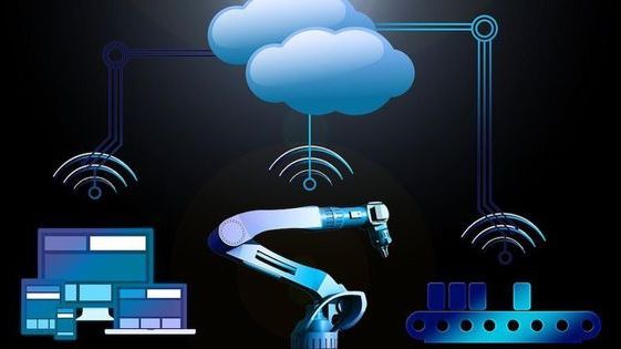
Toggle light / dark theme

Fun in fiction. Perhaps not so much in reality.


The human mind is already pretty open to manipulation—just ask anyone who works in advertising. But neural implant technology could potentially open up a direct digital link to our innermost thoughts that could be exploited by hackers.

In recent months, companies like Elon Musk’s Neuralink, Kernel, and Facebook have unveiled plans to create devices that will provide a two-way interface between human brains and machines.

While these devices could undoubtedly bring many benefits, they would be networked to computers and therefore essentially part of the Internet of Things. That should immediately set off alarm bells for anyone paying attention to cybersecurity news.

We are incredibly excited to announce that Firmamentum, a division of Tethers Unlimited, Inc. (TUI), has signed a contract with the Defense Advanced Research Projects Agency (DARPA) to develop a system that will use in-space manufacturing and robotic assembly technologies to construct on orbit a small satellite able to provide high-bandwidth satellite communications (SATCOM) services to mobile receivers on the ground.

Under the OrbWeaver Direct-to-Phase-II Small Business Innovation Research (SBIR) effort, Firmamentum aims to combine its technologies for in-space recycling, in-space manufacturing, and robotic assembly to create a system that could launch as a secondary payload on an Evolved Expendable Launch Vehicle (EELV). This system would recycle a structural element of that rocket, known as an EELV Secondary Payload Adapter (ESPA) ring, by converting the ring’s aluminum material into a very large, high-precision antenna reflector. The OrbWeaver™ payload would then attach this large antenna to an array of TUI’s SWIFT® software defined radios launched with the OrbWeaver payload to create a small satellite capable of delivering up to 12 gigabits per second of data to K-band very small aperture terminals (VSAT) on the ground.

Read more

Who said Moore’s Law was dead? Certainly not IBM or its chip partners Globalfoundries and Samsung. The trio has developed a transistor manufacturing process that should pave the way for 5-nanometer chips. While the team etched the chip using the same extreme ultraviolet lithography (EUV) used for the breakthrough 7nm chip, it ditched the common FinFET (fin field effect) transistor design in favor of stacks of silicon nanosheets. The switch makes it possible to fine-tune individual circuits to maximize their performance as they’re crammed into an incredibly small space. How small? At 5nm, the group says it can squeeze 30 billion transistors into a chip the size of a fingernail (see below) — not bad when the 7nm chip held 20 billion transistors a couple of years ago.

IBM sees the technique helping its own cognitive computing efforts as well as the Internet of Things and other “data-intensive” tasks. However, it’s also painting a rosy picture for the future of mobile devices — it imagines phones having “two to three times” more battery life than current devices. That’s likely optimistic (phone makers tend to focus on speed over longevity), but it won’t be shocking if future hardware is both faster and wrings out a little more from every charge.

Just don’t expect to see real-world examples of this for a while. We haven’t even seen devices shipping with 7nm chips (they’re not expected until 2018 at the earliest), so it could easily be a couple of years or more before 5nm arrives. Still, that 5nm is even on the roadmap is important. Chip designers won’t have to reinvent the wheel to get meaningful improvements, and you won’t have to worry about device performance growing stale for at least the next few years.

Read more

IBM, its Research Alliance partners Globalfoundries and Samsung, and equipment suppliers have developed an industry-first process to build silicon nanosheet transistors that will enable 5 nanometer (nm) chips. The details of the process will be presented at the 2017 Symposia on VLSI Technology and Circuits conference in Kyoto, Japan. In less than two years since developing a 7nm test node chip with 20 billion transistors, scientists have paved the way for 30 billion switches on a fingernail-sized chip.

The resulting increase in performance will help accelerate cognitive computing, the Internet of Things (IoT), and other data-intensive applications delivered in the cloud. The power savings could also mean that the batteries in smartphones and other mobile products could last two to three times longer than today’s devices, before needing to be charged.

Scientists working as part of the IBM-led Research Alliance at the SUNY Polytechnic Institute Colleges of Nanoscale Science and Engineering’s NanoTech Complex in Albany, NY achieved the breakthrough by using stacks of silicon nanosheets as the device structure of the transistor, instead of the standard FinFET architecture, which is the blueprint for the semiconductor industry up through 7nm node technology.

Read more

The recent efforts to remove Net Neutrality have given many a sense of impending doom we are soon to face. What happens to an Internet without Net Neutrality? Advocates have a vision of the possible results — and it is quite the nightmare! In this segment of Future A to Z, The Galactic Public Archives takes a cheeky, yet compelling perspective on the issue.

Part 1 / Part 2

Follow us on social media:
Twitter / Facebook / Instagram

Individuals who mine Bitcoins needn’t be miners. We call them ‘miners’ because they are awarded BTC as they solve mathematical computations. The competition to unearth these reserve coins also serves a vital purpose. They validate the transactions of Bitcoin users all over the world: buyers, loans & debt settlement, exchange transactions, inter-bank transfers, etc. They are not really miners. They are more accurately engaged in transaction validation or ‘bookkeeping’.

There are numerous proposals for how to incentivize miners once all 21 million coins have been mined/awarded in May 2140. Depending upon the network load and the value of each coin, we may need to agree on an alternate incentive earlier than 2140. At the opening of the 2015 MIT Bitcoin Expo, Andreas Antonopolous proposed some validator incentive alternatives. One very novel suggestion was based on game theory and involved competition and status rather than cash payments.

I envision an alternative approach—one that also addresses the problem of miners and users having different goals. In an ideal world the locus of users should intersect more fully with the overseers…

To achieve this, I have proposed that every wallet be capable of also mining, even if the wallet is simply a smartphone app or part of a cloud account at an exchange service. To get uses participating in validating the transactions of peers, any transaction fee could be waived for anyone who completes 1 validation for each n transactions. (Say one validation for every five or ten transactions). In this manner, everyone pitches in a small amount of resources to maintain a robust network.

A small transaction fee would accrue to anyone who does not participate in ‘mining’ at all. That cost will float with supply and demand. Users can duck the fee by simply participating in the validation process, which continues to be based on either proof-of-work, proof-of-stake — or one of the more exotic proof theories that are being proposed now.

Philip Raymond co-chairs Cryptocurrency Standards Association. He produces
The Bitcoin Event, edits A Wild Duck and is a frequent contributor to Quora

Bitcoin has terrible UX…in our journey into tech we purchased a few pounds worth on a paper wallet on a bitcoin ATM machine to experiment with and gain familiarity with this new form of internet money.

The paper wallet has an illegibly long code that needs to be typed in or QR code scanned in to get the part bitcoin uploaded to an online usable form of bitcoin.

Bitcoins can be lost because of this bad UX/UI issue.

Read more

Wi-Fi can pass through walls. This fact is easy to take for granted, yet it’s the reason we can surf the web using a wireless router located in another room.

However, not all of that microwave radiation makes it to or from our phones, tablets, and laptops. Routers scatter and bounce their signal off objects, illuminating our homes and offices like invisible light bulbs.

Now, German scientists have found a way to exploit this property to take holograms, or 3D photographs, of objects inside of a room — from outside of the room.

Read more

Confidential details of a top-secret encryption-breaking supercomputer were left completely exposed on an unsecured computer server belonging to New York University (NYU), according to a new report.

While it’s not uncommon for even critical-level infrastructure to suffer potentially catastrophic security breaches, what makes this event different is that there was seemingly no foul-play or attempts to hack into NYU’s systems.

Instead, it looks like somebody may have just forgotten to secure their classified data properly, exposing hundreds of pages of information on a covert code-breaking machine co-administered by the Department of Defence, IBM, and NYU.

Read more