Archive for the ‘electronics’ category: Page 84
Apr 6, 2016
Samsung Files Patent For Augmented Reality Smart Contact Lenses
Posted by Karen Hurst in categories: augmented reality, electronics, mobile phones, transportation
Samsung’s dream of creating smart contact lenses capable of capturing images and shooting videos has just drawn closer. However, the patent reveals that Samsung has been working on the concepts and not necessarily the actual product which they trademarked as Gear Blink, which was filed in both South Korea and the U.S.
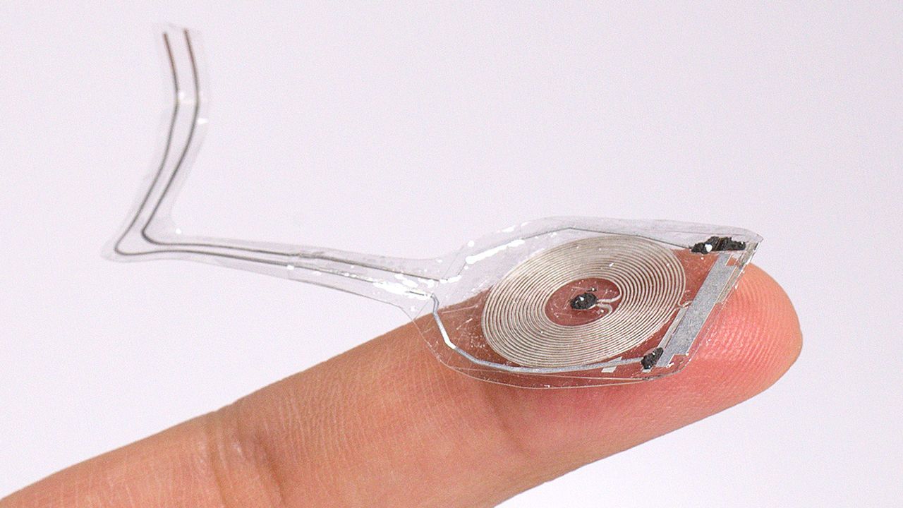
‘The analysis component of the contact lens can process the raw image data of the camera to determine processed image data indicating that the blind person is approaching intersection with a crosswalk and establish that there is a vehicle approaching the intersection’. It could very well be a smart contact lens. It’s a contact lens that consists of a small display, camera, RF antenna, and sensors to detect eye movement.
SamMobile states that the “lenses can provide a more natural way to provide augmented reality than smart glasses”. While the display projects images directly into the eye of the person wearing the contacts, an external device like a smartphone is needed for processing.
Continue reading “Samsung Files Patent For Augmented Reality Smart Contact Lenses” »
Apr 6, 2016
Samsung granted patent for smart contact lenses with a tiny camera
Posted by Klaus Baldauf in category: electronics
In an ever expanding universe of wearables, Samsung is doing its best to keep all bases covered. Today, the publication of a patent application shows the company is developing smart contact lenses.
The patent application, filed in South Korea, shows a contact lens equipped with a tiny display, a camera, an antenna, and several sensors that detect movement and the most basic form of input using your eyes: blinking.
Continue reading “Samsung granted patent for smart contact lenses with a tiny camera” »
Apr 5, 2016
Changing the color of single photons in a diamond quantum memory
Posted by Karen Hurst in categories: computing, electronics, quantum physics
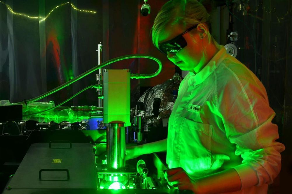
Researchers from the Institute for Quantum Computing at the University of Waterloo and the National Research Council of Canada (NRC) have, for the first time, converted the colour and bandwidth of ultrafast single photons using a room-temperature quantum memory in diamond.
Shifting the colour of a photon, or changing its frequency, is necessary to optimally link components in a quantum network. For example, in optical quantum communication, the best transmission through an optical fibre is near infrared, but many of the sensors that measure them work much better for visible light, which is a higher frequency. Being able to shift the colour of the photon between the fibre and the sensor enables higher performance operation, including bigger data rates.
Continue reading “Changing the color of single photons in a diamond quantum memory” »
Apr 5, 2016
World’s Smallest Diode Is Made of DNA
Posted by Shailesh Prasad in categories: biotech/medical, computing, electronics, genetics
Diodes —also known as rectifiers—allow electric current to flow in just one direction. More than 40 years ago, scientists proposed miniaturizing diodes and other electronic components down to the size of single molecules, an idea that eventually helped give birth to the field of molecular electronics, which could help push computing beyond the limits of conventional silicon devices. [See “Whatever Happened to the Molecular Computer?” IEEE Spectrum, October 2015]
Scientists at the University of Georgia and Ben-Gurion University of the Negev in Israel used DNA to fashion the new diode. The breakthroughs in genetics developed to sequence the human genome have now made it relatively easy to precisely manufacture and manipulate DNA, which makes the molecule a leading candidate for use in molecular electronics.
DNA’s double helix is made of paired strands of molecules known as bases. The new diode is only 11 base pairs long. (Typically, DNA is 0.34 nanometers long per base pair.)
Apr 4, 2016
ORNL 20kW wireless charging system hits 90% efficiency
Posted by Shailesh Prasad in categories: electronics, energy, engineering, transportation
Oak Ridge National Laboratory (ORNL) has been working on a wireless charging system for EVs and plug-in hybrids for years. The goal is to create a system that makes charging EVs and hybrids easier for drivers and to make EVs and other plug-in vehicles as cheap and easy to own as a gasoline vehicle. ORNL has announced that it has demonstrated a 20-kilowatt wireless charging system that has achieved 90% efficiency at three times the rate of the plug-in systems commonly used in electric cars today.
ORNL has multiple industry partners that are participating in this program including Toyota, Cisco Systems, Evatran, and Clemson University International Center for Automotive Research. “We have made tremendous progress from the lab proof-of-concept experiments a few years ago,” said Madhu Chinthavali, ORNL Power Electronics Team lead. “We have set a path forward that started with solid engineering, design, scale-up and integration into several Toyota vehicles. We now have a technology that is moving closer to being ready for the market.”
Continue reading “ORNL 20kW wireless charging system hits 90% efficiency” »
Apr 1, 2016
Successfully Engineering Water-loving Nanoparticle Diodes
Posted by Shailesh Prasad in categories: computing, electronics, engineering
Nanoparticle diodes and devices that work when wet.
“Groundbreaking” research by Prof. Bartosz Grzybowski (School of Natural Science).
Nanoparticle Diodes and Devices That Work When Wet.
A new study by an international team of researchers, affiliated with UNIST has found a new way to produce electronic devices, such as diodes, logic gates, and sensors without the need of semiconductors.
Continue reading “Successfully Engineering Water-loving Nanoparticle Diodes” »
Mar 29, 2016
New plasma printing technique can deposit nanomaterials on flexible, 3D substrates
Posted by Karen Hurst in categories: computing, electronics, nanotechnology, wearables
A new nanomaterial printing method could make it both easier and cheaper to create devices such as wearable chemical and biological sensors, data storage and integrated circuits — even on flexible surfaces such as paper or cloth. The secret? Plamsa.
Mar 29, 2016
Multiple bends won’t crack this lightweight, paper-like, flexible ceramic
Posted by Klaus Baldauf in categories: electronics, materials, wearables
A flexible, paper-like ceramic material has been created that promises to provide an inexpensive, fireproof, non-conductive base for a whole range of new and innovative electronic devices (Credit: Eurakite). View gallery (4 images)
Materials to make hard-wearing, bendable non-conducting substrates for wearables and other flexible electronics are essential for the next generation of integrated devices. In this vein, researchers at the University of Twente have reformulated ceramic materials so that they have the flexibility of paper and the lightness of a polymer, but still retain exceptional high-temperature resistance. The new material has been dubbed flexiramics.
Continue reading “Multiple bends won’t crack this lightweight, paper-like, flexible ceramic” »