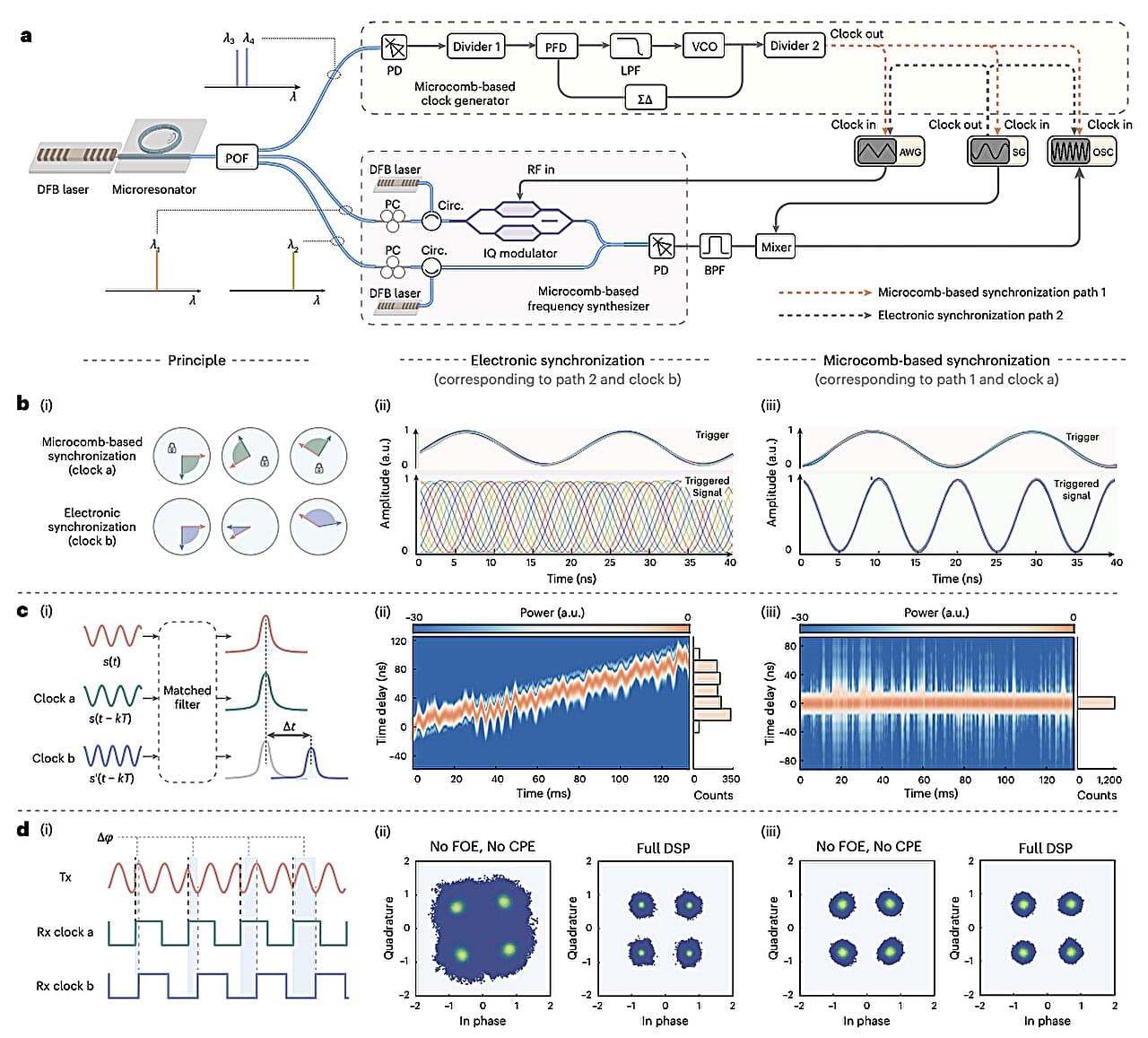
Toggle light / dark theme

Novel quantum sensor breaks limits of optical measurement using entanglement

The Korea Research Institute of Standards and Science (KRISS) has developed a novel quantum sensor technology that allows the measurement of perturbations in the infrared region with visible light by leveraging the phenomenon of quantum entanglement. This will enable low-cost, high-performance IR optical measurement, which previously accompanied limitations in delivering quality results.

Powering Next-Gen Electronics: Scientists Find High-Performance Alternative to Conventional Ferroelectrics

Lighting a gas grill, getting an ultrasound, using an ultrasonic toothbrush ⎯ these actions involve the use of materials that can translate an electric voltage into a change in shape and vice versa.

Known as piezoelectricity, the ability to trade between mechanical stress and electric charge can be harnessed widely in capacitors, actuators, transducers, and sensors like accelerometers and gyroscopes for next-generation electronics. However, integrating these materials into miniaturized systems has been difficult due to the tendency of electromechanically active materials to ⎯ at the submicrometer scale, when the thickness is just a few millionths of an inch ⎯ get “clamped” down by the material they are attached to, which significantly dials down their performance.

Rice University researchers and collaborators at the University of California, Berkeley have found that a class of electromechanically active materials called antiferroelectrics may hold the key to overcoming performance limitations due to clamping in miniaturized electromechanical systems. A new study published in Nature Materials reports that a model antiferroelectric system, lead zirconate (PbZrO3), produces an electromechanical response that can be up to five times greater than that of conventional piezoelectric materials even in films that are only 100 nanometers (or 4 millionths of an inch) thick.

Researchers create the world’s strongest ionizing terahertz radiation

Lying between the microwave and infrared regions of the electromagnetic spectrum, the terahertz (1 THz = 10¹² Hz) gap is being rapidly closed by development of new terahertz sources and detectors, with promising applications in spectroscopy, imaging, sensing, and communication.

These applications greatly benefit from terahertz sources delivering high-energy or high-average-power radiation. On the other hand, high-intensity or strong-field terahertz sources are essential to observe or exploit novel nonlinear terahertz-matter interactions, where the electric and/or magnetic field strengths play a key role.

The team of scientists, led by Dr. Chul Kang from Advanced Photonics Research Institute, Gwangju Institute of Science and Technology (GIST), Korea, and Professor Ki-Yong Kim from Institute for Research in Electronics and Applied Physics, University of Maryland, College Park, Maryland, U.S., has created the world’s strongest terahertz fields of 260 megavolts per centimeter (MV/cm) or equivalent peak intensity of 9 × 10¹³ watts per square centimeter (W/cm²).

Semiconductor advancement could lead to low-cost, flexible electronic devices

The public’s appetite for inexpensive and powerful electronic devices continues to grow. While silicon-based semiconductors have been key to satiating this demand, a superior alternative could be wide-bandgap semiconductors. These materials, which operate at higher temperatures and handle increased power loads, are unfortunately very expensive.

Expanding on the fundamental principles of liquid movement

From the rain drops rolling down your window, to the fluid running through a COVID rapid test, we cannot go a day without observing the world of fluid dynamics. Naturally, how liquids traverse across, and through, surfaces is a heavily researched subject, where new discoveries can have profound effects in the fields of energy conversion technology, electronics cooling, biosensors, and micro-/nano-fabrications.

Revolutionizing Photonics: 2D Materials Manipulate Light With Remarkable Precision

NYU Abu Dhabi researchers have unveiled a novel 2D material improving optical modulation for advanced systems and communications.

Responding to the increasing demand for efficient, tunable optical materials capable of precise light modulation to create greater bandwidth in communication networks and advanced optical systems, a team of researchers at NYU Abu Dhabi’s Photonics Research Lab (PRL) has developed a novel, two-dimensional (2D) material capable of manipulating light with exceptional precision and minimal loss.

Tunable optical materials (TOMs) are revolutionizing modern optoelectronics, electronic devices that detect, generate, and control light. In integrated photonics circuits, precise control over the optical properties of materials is crucial for unlocking groundbreaking and diverse applications in light manipulation. Two-dimensional materials like Transition Metal Dichalcogenides (TMDs) and graphene exhibit remarkable optical responses to external stimuli. However, achieving distinctive modulation across a short-wave infrared (SWIR) region while maintaining precise phase control at low signal loss within a compact footprint has been a persistent challenge.

/* */