Another version of the PCP theorem, not yet proved, specifically deals with the quantum case. Computer scientists suspect that the quantum PCP conjecture is true, and proving it would change our understanding of the complexity of quantum problems. It’s considered arguably the most important open problem in quantum computational complexity theory. But so far, it’s remained unreachable.
Nine years ago, two researchers identified an intermediate goal to help us get there. They came up with a simpler hypothesis, known as the “no low-energy trivial state” (NLTS) conjecture, which would have to be true if the quantum PCP conjecture is true. Proving it wouldn’t necessarily make it any easier to prove the quantum PCP conjecture, but it would resolve some of its most intriguing questions.
Then in June of 2022, in a paper posted to the scientific preprint site arxiv.org, three computer scientists proved the NLTS conjecture. The result has striking implications for computer science and quantum physics.
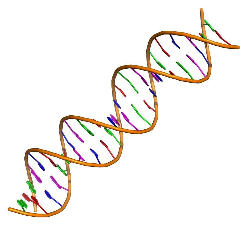
DNA-based information is a new interdisciplinary field linking information technology and biotechnology. The field hopes to meet the enormous need for long-term data storage by using DNA as an information storage medium. Despite DNA’s promise of strong stability, high storage density and low maintenance cost, however, researchers face problems accurately rewriting digital information encoded in DNA sequences.
Generally, DNA data storage technology has two modes, i.e., the “in vitro hard disk mode” and the “in vivo CD mode.” The primary advantage of the in vivo mode is its low-cost, reliable replication of chromosomal DNA by cell replication. Due to this characteristic, it can be used for rapid and low-cost data copy dissemination. Since encoded DNA sequences for some information contain a large number of repeats and the appearance of homopolymers, however, such information can only be “written” and “read,” but cannot be accurately “rewritten.”
To solve the rewriting problem, Prof. Liu Kai from the Department of Chemistry, Tsinghua University, Prof. LI Jingjing from the Changchun Institute of Applied Chemistry (CIAC) of the Chinese Academy of Sciences, and Prof. Chen Dong from Zhejiang University led a research team that recently developed a dual-plasmid editing system for accurately processing digital information in a microbial vector. Their findings were published in Science Advances.
The World Meteorological Organization (WMO) states that there’s a 93 percent chance that one year between now and 2026 will be the hottest on record. Not only will these record high temperatures have an impact on our environment and lives, but they are also expected to change the way in which we safeguard technology. For example, how do you cool data centers while the outside temperature keeps getting higher and higher?
This problem has been discussed previously before due to several failings of data centers around the world caused by cooling failures. That weather shift will have an impact on all human-made infrastructure—including the data centers that keep our planet’s collective knowledge online. According to wired.com, 45 percent of US data centers have experienced an extreme weather event that threatened their ability to operate.
When users want to send data over the internet faster than the network can handle, congestion can occur—the same way traffic congestion snarls the morning commute into a big city.
Computers and devices that transmit data over the internet break the data down into smaller packets and use a special algorithm to decide how fast to send those packets. These congestion control algorithms seek to fully discover and utilize available network capacity while sharing it fairly with other users who may be sharing the same network. These algorithms try to minimize delay caused by data waiting in queues in the network.
Over the past decade, researchers in industry and academia have developed several algorithms that attempt to achieve high rates while controlling delays. Some of these, such as the BBR algorithm developed by Google, are now widely used by many websites and applications.
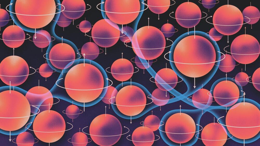
Using just a handful of quantum bits, researchers have used a quantum computer to simulate an infinite line of electron-like particles. The technique could be used to better understand the behaviour of molecules in materials.
Computer-based animators who are tasked with bringing to life imaginary worlds and characters are aided by simulators that can model the many possible ways an object or fluid might move through a physical space. Known as “solvers,” these simulators provide a significant head start on the work of animation. But there’s a catch. As computers have gotten faster, these solvers often create too many options for the animator to effectively sort through looking for just the right one.
“A simulator can return thousands of options. It’s so time consuming to sort through them that these helpful solvers can’t be used to their full potential,” said Purvi Goel, a doctoral candidate in computer science at Stanford, who with her mentor, professor Doug James, has created a new approach to refine the search and narrow results to the most promising options.
They call it “Unified Many-Worlds Browsing,” and they will debut their approach at the upcoming SIGGRAPH 2022 conference in Vancouver, British Columbia, the premier annual gathering for computer graphics and interactive techniques. The approach could both speed the search process for animators and, by limiting the options the simulators must cycle through, reduce compute time and expense. Ultimately, the researchers hope, it will allow artists and scientists to interface with solvers with unparalleled ease and efficiency.
Innovative Solutions For Unmet Needs Of Older Adults & Their Caregivers — Keith Camhi, Managing Director, Techstars Future of Longevity Accelerator — A Partnership With Melinda Gates Pivotal Ventures.
Keith Camhi is Managing Director, Techstars Future of Longevity Accelerator (https://www.techstars.com/accelerators/longevity), a program, run in partnership with Pivotal Ventures (https://www.pivotalventures.org/), an investment and incubation company created by Melinda French Gates, focusing on innovative solutions to address the unmet needs of older adults and their caregivers. The longevity accelerator core program themes include: Caregiver Support, Care Coordination, Aging in Place, Financial Wellness and Resilience, Preventive Health (both Physical and Cognitive), and Social Engagement.
Keith was previously the SVP of Accelerators for Techstars globally and was inspired to move to the MD role for the longevity program based on having built a venture-backed startup serving older adults himself, having experienced the gaps in America’s care giving infrastructure firsthand, and wanting to support entrepreneurs who are building solutions to address this substantial market opportunity.
Techstars is a global investment business that provides access to capital, one-on-one mentorship, a worldwide network and customized programming for early-stage entrepreneurs. It was founded in 2006 in Boulder, Colorado. As of May 2022, the company had accepted over 2,900 companies into its accelerator programs with a combined market capitalization of US$71 billion.
Prior to Techstars, Keith founded and led the rapid growth of two tech companies in the health and fitness industry – one that reached #20 on the Deloitte Fast 500, and another that made Entrepreneur’s Franchise 500 three times. He has raised over $50 million in venture funding, holds several patents for sensor and machine vision technology, has been an angel investor and LP in several venture funds, and enjoys mentoring promising startups.
Unlike the moon’s surface, which heats up to 260 degrees Fahrenheit (127 degrees Celsius) during the day and drops to minus 280 degrees Fahrenheit (minus 173 degrees Celsius) at night, these lunar pits in the Mare Tranquillitatis region have a human-friendly, stable temperature.
(Mare Tranquillitatis, commonly known as the Sea of Tranquility, is where Apollo 11, the first mission to put humans on the moon, landed due to its smooth and relatively flat terrain.)
The data comes from an analysis of images taken by NASA’s Lunar Reconnaissance Orbiter spacecraft and computer modeling.
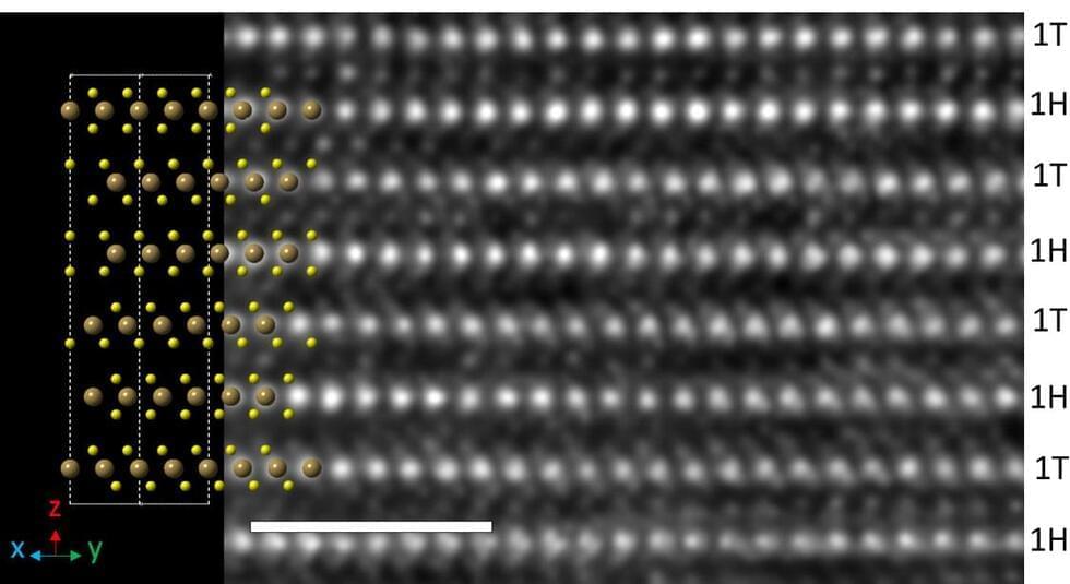
Scientists from The University of Manchester have developed a novel yet simple method for producing vertical stacks of alternating superconductor and insulator layers of tantalum disulphide (TaS 2). The findings, from a team led by Professor Rahul Nair, could speed up the process of manufacturing such devices – so-called van der Waals heterostructures – with application in high-mobility transistors, photovoltaics and optoelectronics.
Van der Waals heterostructures are much sought after since they display many unique and useful properties not found in naturally occurring materials. In most cases, they are prepared by manually stacking one layer over the other in a time-consuming and labour-intensive process.
Electron microscopy image of the synthesized 6R TaS 2 with an atomic model of the material on the left. The brown spheres represent Ta atoms and the yellow spheres represent sulphur atoms. The atomic positions and arrangement in the microscopic image are an exact match with the model, confirming its structure. (Image: University of Manchester)

 עברית (Hebrew)