Scientists have uploaded a viral genome to a quantum computer, marking an important step for the future of quantum-enabled advancements in biology.
Category: computing – Page 6
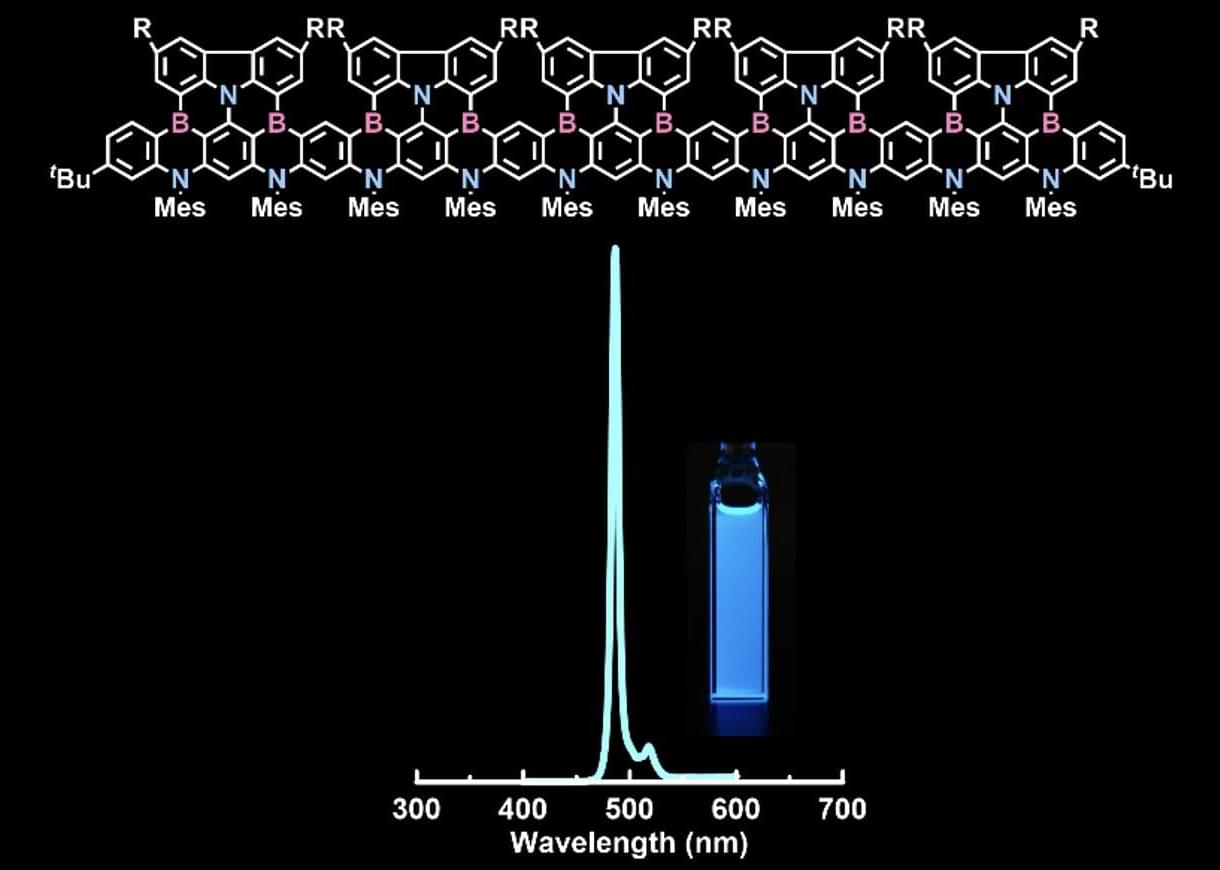
Organic molecule with ultranarrow emission spectrum could lead to better LEDs
Over the past several decades, light sources have gradually transitioned to light-emitting diodes, or LEDs, and inorganic LEDs are now used across a wide range of applications. In parallel, organic LEDs, or OLEDs, have become widely used in display technologies.
OLEDs in particular offer significant advantages in devices such as smartphones, including higher resolution and lower power consumption. All LEDs operate based on spontaneous emission, which is inherently broadband, and OLEDs in particular produce broad emission spectra.
Narrowing this spontaneous emission toward a monochromatic limit would greatly increase its utility, a goal that has long been a central pursuit in photonics. For example, a narrower emission would achieve more highly saturated colors in LED-based displays.
Majorana modes withstand disorder in atomic chains, boosting fault-tolerant quantum computing
Quantum computers—systems that process information and perform computations by leveraging the principles of quantum mechanics—could solve some tasks faster and more effectively than classical computers. While some studies have demonstrated the advantages of these computers for specific tasks, ensuring their reliable operation in real-world settings has proved challenging.
This is partly because quantum information units, or qubits, are known to be highly sensitive to environmental disturbances, such as fluctuations in temperature, electromagnetic fluctuations and magnetic fields. These environmental disturbances, collectively referred to as “noise,” can alter the qubit’s delicate quantum states, leading to computational errors.
In recent years, quantum physicists and engineers have proposed various strategies that could protect qubits from environmental disturbances and reduce quantum computing errors. One proposed solution is to rely on Majorana modes.
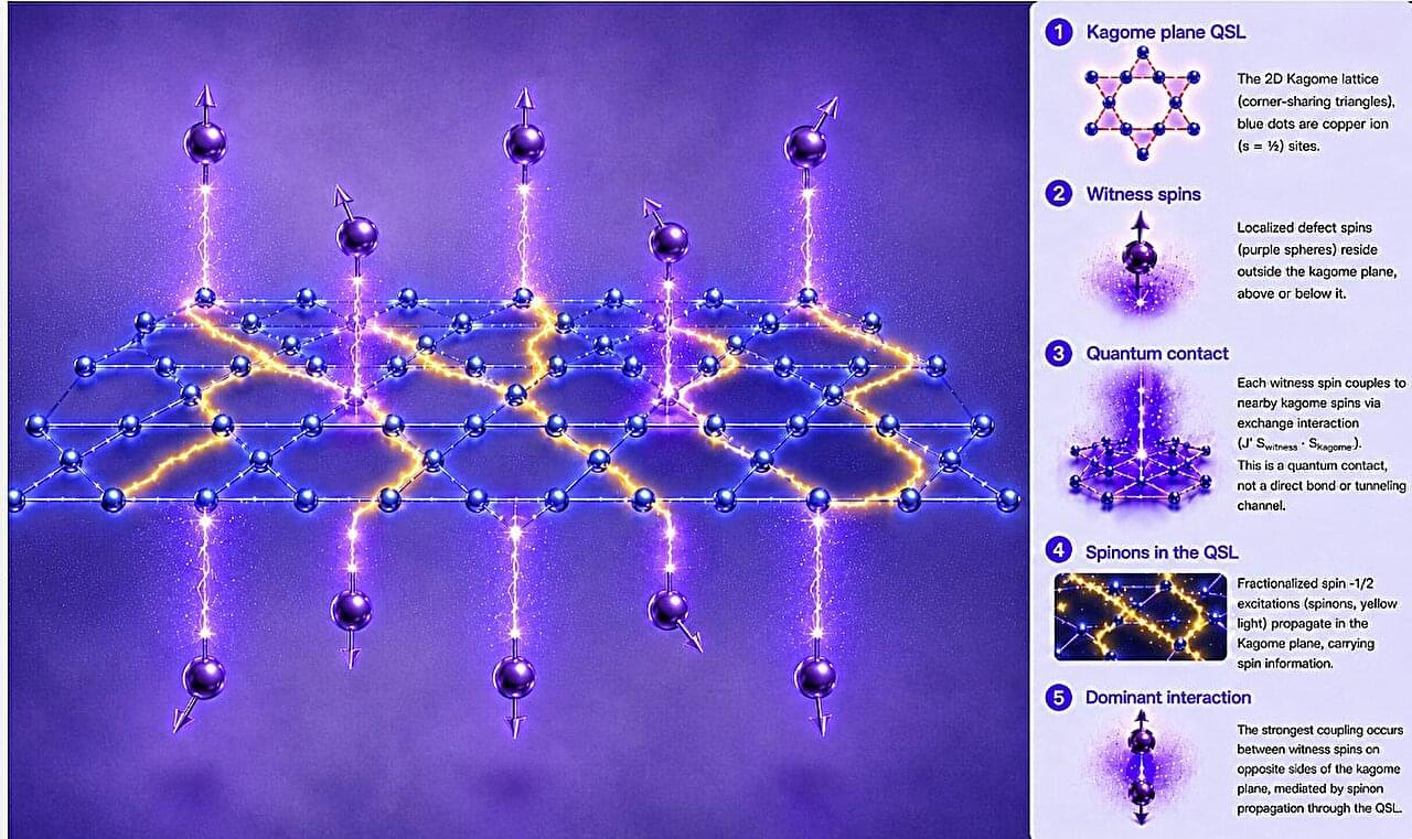
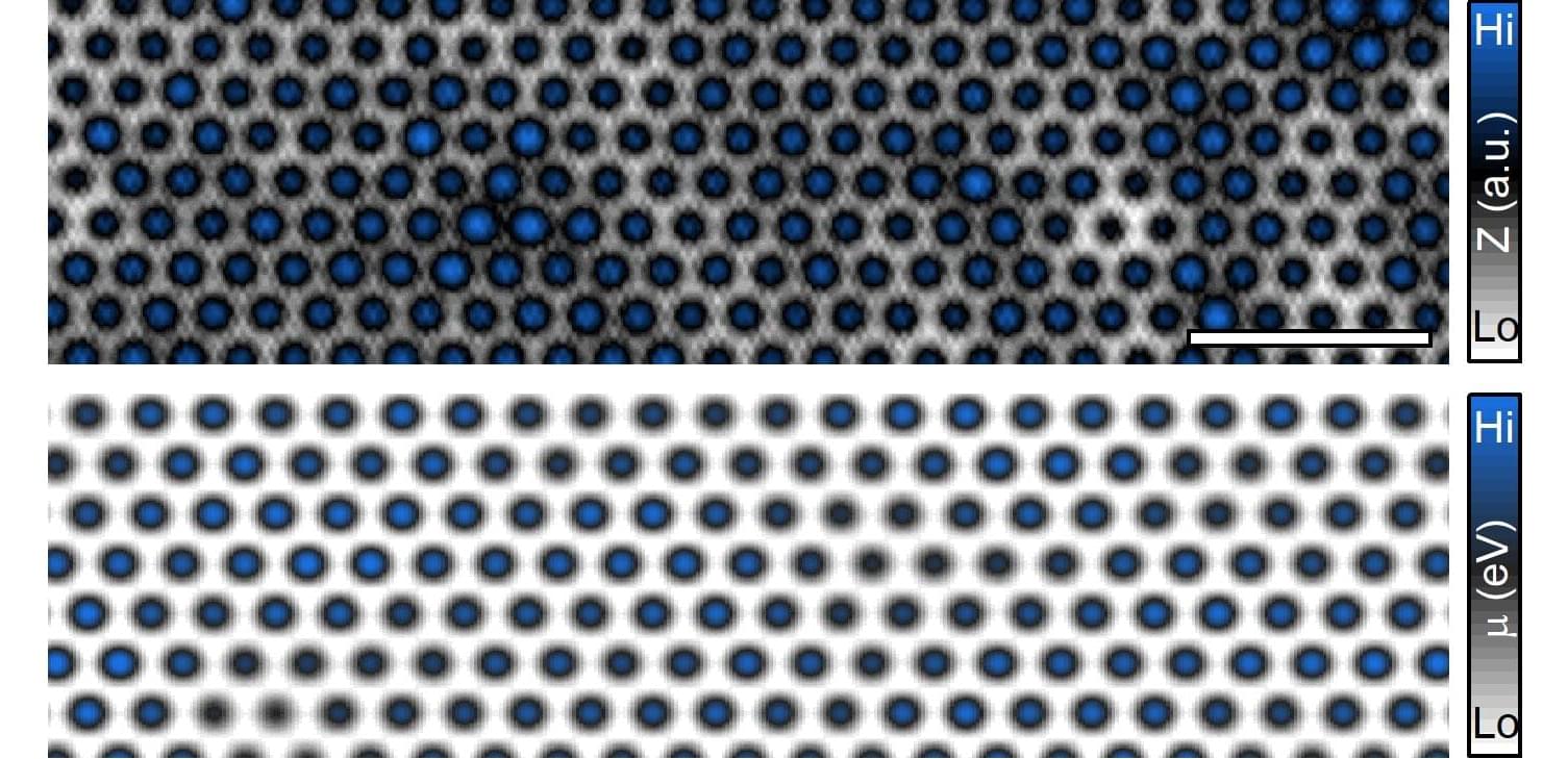
Quantum witness technique reveals spinons in quantum spin liquid candidate
Physicists at University College Cork have developed a new approach in the search for a quantum spin liquid, a long-sought state of quantum matter resembling a magnetic liquid whose quantum properties mean it never freezes. The work is a key step in the search for quantum silicon, a mineral that could be used to create quantum computers, just as silicon is used in traditional computers. The resulting paper appears in Nature Physics.
Lead author Prof. Seamus Davis said, “By introducing the quantum witness technique we provide a completely new perspective on the physics of quantum spin liquids and access their internal quantum excitations or ‘spinons’ directly for the first time at UCC.”
As liquids cool, they freeze into solids as their atoms cease to move. But some liquids, such as helium, never freeze. Predominant quantum effects mean they flow as superfluids even at absolute zero (the coldest possible temperature).
Xanadu’s photonic approach to quantum computing
Enjoy the videos and music you love, upload original content, and share it all with friends, family, and the world on YouTube.
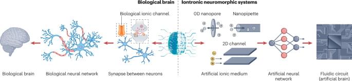
Nanofluidic ionic memory for next-generation computing
In the brain, memory involves release of neurotransmitters and transport of ions through nanoconfined channels. This Perspective discusses how nanofluidic memristors emulate this confined ion transport, highlighting the materials, design strategies and challenges involved in developing brain-inspired computing technologies.
Dino-killing asteroid may have fueled underground life for 8 million years
The asteroid that caused the extinction of the dinosaurs also created an underground environment suited to supporting new life, and new research suggests it lasted for millions of years longer than previously suspected.
The finding has surprised the international team of researchers behind it, who came to their conclusions by pairing sophisticated new analysis of samples taken from the Chicxulub crater in Mexico with computer modeling of the geological effects of the asteroid impact that formed the crater 66 million years ago.
The research, published in the journal Communications Earth & Environment, casts new light on how life may have first been incubated in hydrothermal systems in the earliest chapters of Earth’s history and could help direct the search for life on other planets.
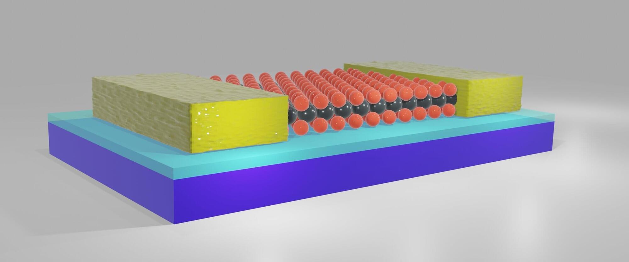
Monolayer WSe₂ unlocks high-performance p-type transistors that could change how future chips balance speed and power
Transistors, small devices that can amplify or switch electrical signals, are central components of all modern computer chips and digital devices. There are two main types of transistors, known as n-type and p-type transistors.
N-type transistors conduct current using electrons (i.e., negatively charged particles), while p-type transistors utilize electron holes (i.e., positively charged spaces in a crystal lattice without electrons).
Electronics engineers worldwide have been exploring different solutions that could help reduce the size of existing transistors without compromising their performance, which could enable the further miniaturization of electronic devices. One promising route is to fabricate transistors using two-dimensional (2D) semiconductors, semiconducting materials that are just a single atom or a few atoms thick.