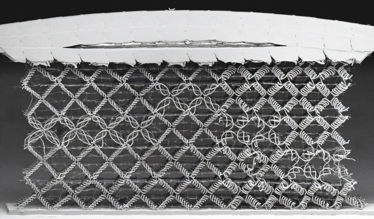
Toggle light / dark theme

Scientists create scalable quantum node linking light and matter

Quantum scientists in Innsbruck have taken a major leap toward building the internet of the future. Using a string of calcium ions and finely tuned lasers, they created quantum nodes capable of generating streams of entangled photons with 92% fidelity. This scalable setup could one day link quantum computers across continents, enable unbreakable communication, and even transform timekeeping by powering a global network of optical atomic clocks that are so precise they’d barely lose a second over the universe’s entire lifetime.

Quantum ‘curvature’ warps electron flow, hinting at new electronics possibilities

How can data be processed at lightning speed, or electricity conducted without loss? To achieve this, scientists and industry alike are turning to quantum materials, governed by the laws of the infinitesimal. Designing such materials requires a detailed understanding of atomic phenomena, much of which remains unexplored.

A team from the University of Geneva (UNIGE), in collaboration with the University of Salerno and the CNR-SPIN Institute (Italy), has taken a major step forward by uncovering a hidden geometry—until now purely theoretical—that distorts the trajectories of electrons in much the same way gravity bends the path of light. The work, published in Science, opens new avenues for .

Future technologies depend on high-performance materials with unprecedented properties, rooted in quantum physics. At the heart of this revolution lies the study of matter at the microscopic scale—the very essence of . In the past century, exploring atoms, electrons and photons within materials gave rise to transistors and, ultimately, to modern computing.

Scientists Build Quantum Computer That Snaps Together Like LEGOs

A modular quantum processor design shows ~99% fidelity. It paves the way for scalable quantum computing. What do children’s building blocks and quantum computing have in common? The answer is modularity. Constructing a quantum computer as a single, unified device proves extremely difficult. Th

Integrated lithium niobate photonic computing circuit based on efficient and high-speed electro-optic conversion

Efficient electro-optic conversion is central to photonic computing, and thin-film lithium niobate (TFLN) offers this capability. Here, the authors demonstrate computing circuits on the TFLN platform, enabling the next generation of photonic computing systems featuring both high-speed and low-power.

Starship IFT-10 & Starlink

SpaceX’s successful Starship IFT-10 test and advancements in Starlink technology are poised to significantly reduce launch costs and disrupt the broadband landscape, paving the way for a more efficient and cost-effective space travel and satellite internet service.

## Questions to inspire discussion.

Starship and Starlink Advancements.

🚀 Q: How does Starship improve Starlink satellite deployment? A: Starship enables deployment of V3 Starlink satellites that are 40-50X cheaper per unit bandwidth compared to Falcon 9, according to Mach33 research.

📡 Q: What advantages do larger satellites on Starship offer? A: Starship’s size allows for larger satellites delivering more bandwidth per mass, improving physics scaling laws and making it 50X more efficient than Falcon 9 for launching bandwidth per kilogram.

Cost and Capacity Improvements.

Scientists create realistic brain-wide connection maps through digital modeling

EPFL researchers have developed a powerful method to generate brain-wide, biologically realistic wiring maps of the mouse brain. Their approach bridges experimental data with mathematical and computational modeling to simulate how neurons connect across the entire brain.

The study is published in the journal Nature Communications.

One of neuroscience’s greatest challenges is understanding how the brain is wired. Even with modern imaging tools, it has been a challenge to create detailed maps that show how the brain’s billions of cells () connect, not just with their local “neighbors” but also to other, more distant cells in the brain.

Interface-controlled antiferromagnetic tunnel junctions offer new path for next-gen spintronics

A research team led by Prof. Shao Dingfu at the Institute of Solid State Physics, the Hefei Institutes of Physical Science of the Chinese Academy of Sciences, has unveiled a new mechanism for achieving strong spin polarization using antiferromagnetic metal interfaces.

Their findings, published in Newton recently, propose a third prototype of antiferromagnetic tunnel junction (AFMTJ), paving the way for faster and denser spintronic devices.

As electronics demand smaller size, higher speed, and lower energy use, spintronics—using both electron charge and spin—offers a strong alternative to traditional devices. Magnetic tunnel junctions (MTJs), a key spintronics technology, are already used in but face limits due to slow response speeds and unwanted magnetic fields from their ferromagnetic parts.

Optoelectronics research could bring holograms to your smartphone and closer to everyday use

New research from the University of St Andrews paves the way for holographic technology, with the potential to transform smart devices, communication, gaming and entertainment.

In a study published in Light: Science & Applications, researchers from the School of Physics and Astronomy created a new optoelectronic device from the combined use of holographic metasurfaces (HMs) and (OLEDs).

Until now, holograms have been created using lasers. However, researchers have found that using OLEDs and HMs gives a simpler and more compact approach that is potentially cheaper and easier to apply, overcoming the main barriers to hologram technology being used more widely.

/* */