Watch out qubits!
Scientists successfully measure high-dimensional qudits, cousins to quantum computing qubits.


Here’s a nice article discussing the progress of the brain-computer interface industry, some existing startups in the space, and where the industry may go in the future.
Fifty years after the term brain–computer interface was coined, the neurotechnology is being pursued by an array of start-up companies using a variety of different technologies. But the path to clinical and commercial success remains uncertain.

Loongson has revealed that its next-gen CPUs will be able to match Intel’s 12th Gen Core i7 & Core i5 CPUs, propelling the domestic Chinese PC market to new heights.
Loongson CEO States Up To 50% Performance Increase Possible On Next-Gen 8-Core CPUs, Reaching Intel 12th Gen Levels
During an interview with Loongson’s CEO, Hu Weiwu, with local Chinese media, it was highlighted that the upcoming CPUs from the chipmaker are going to be a major upgrade. Currently, Loongson offers its 8-core 3A6000 CPU which offers performance close to Intel’s 10th Gen & AMD’s Zen 2 core architectures. The company also recently previewed its 3B6600 and 3B7000 CPUs for PCs that use an 8-core design and are built on the same process node as the 3A6000 CPUs.

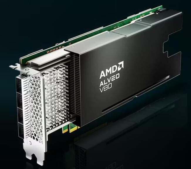
AMD has announced mass production of its Alveo V80 compute accelerator, the firm’s newest HPC product targeted at memory-intensive workloads.
AMD’s Alveo V80 Targets Memory-Intensive HPC Workloads Through Heterogeneous Integration Courtesy of Versal HBM
The Alveo V80 was a silent announcement by AMD, but it does indeed pack a punch. This card targets catering to mid-tier workloads that are heavily dependent on memory utilization and expects to witness massive adoption in the fields of HPC, Networking, and Storage Applications. The FPGA-based accelerator looks to make strides in the industry through its competitive performance and the price tag it comes with, which we’ll discuss later.


A recent United Nations report found that the world generated 137 billion pounds of electronic waste in 2022, an 82% increase from 2010. Yet less than a quarter of 2022’s e-waste was recycled. While many things impede a sustainable afterlife for electronics, one is that we don’t have systems at scale to recycle the printed circuit boards (PCBs) found in nearly all electronic devices.
PCBs — which house and interconnect chips, transistors and other components — typically consist of layers of thin glass fiber sheets coated in hard plastic and laminated together with copper. That plastic can’t easily be separated from the glass, so PCBs often pile up in landfills, where their chemicals can seep into the environment. Or they’re burned to extract their electronics’ valuable metals like gold and copper. This burning, often undertaken in developing nations, is wasteful and can be toxic — especially for those doing the work without proper protections.
A team led by researchers at the University of Washington developed a new PCB that performs on par with traditional materials and can be recycled repeatedly with negligible material loss. Researchers used a solvent that transforms a type of vitrimer — a cutting-edge class of sustainable polymers — to a jelly-like substance without damaging it, allowing the solid components to be plucked out for reuse or recycling.

Researchers have developed a new communication paradigm that can let them securely connect a PC to a quantum computer over the internet.
Known as “blind quantum computing,” the technique uses a fiber-optic cable to connect a quantum computer with a photon-detecting device and uses quantum memory — the equivalent of conventional computing memory for quantum computers. This device is connected directly to a PC, which can then perform operations on the quantum computer remotely. The details were outlined in a new study published April 10 in the journal Physical Review Letters.
🔒 Keep Your Digital Life Private and Be Safe Online: https://nordvpn.com/safetyfirst…
