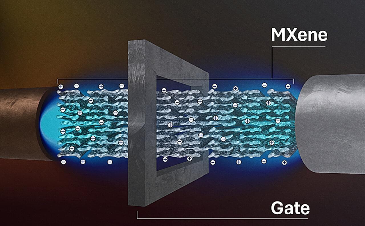
By applying voltage to electrically control a new “transistor” membrane, researchers at Lawrence Livermore National Laboratory (LLNL) achieved real-time tuning of ion separations—a capability previously thought impossible. The recent work, which could make precision separation processes like water treatment, drug delivery and rare earth element extraction more efficient, was published in Science Advances.
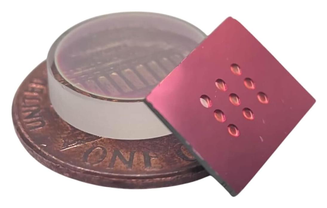
The membranes are made of stacks of MXenes —2D sheets that are only a few atoms thick. Ions squeeze through nanoscale channels formed in the gaps between the stacked MXene layers.
Until now, scientists thought MXene membrane properties were intrinsic and unchangeable once created. The rate of ion transport was thought to be baked in from the beginning.