UK’s first 100-qubit quantum computer and a submarine-tested atomic clock now anchor Infleqtion’s new Oxford centre, tripling local R&D and production.

Investigadores enseñan a las células cerebrales a jugar a ‘Doom’
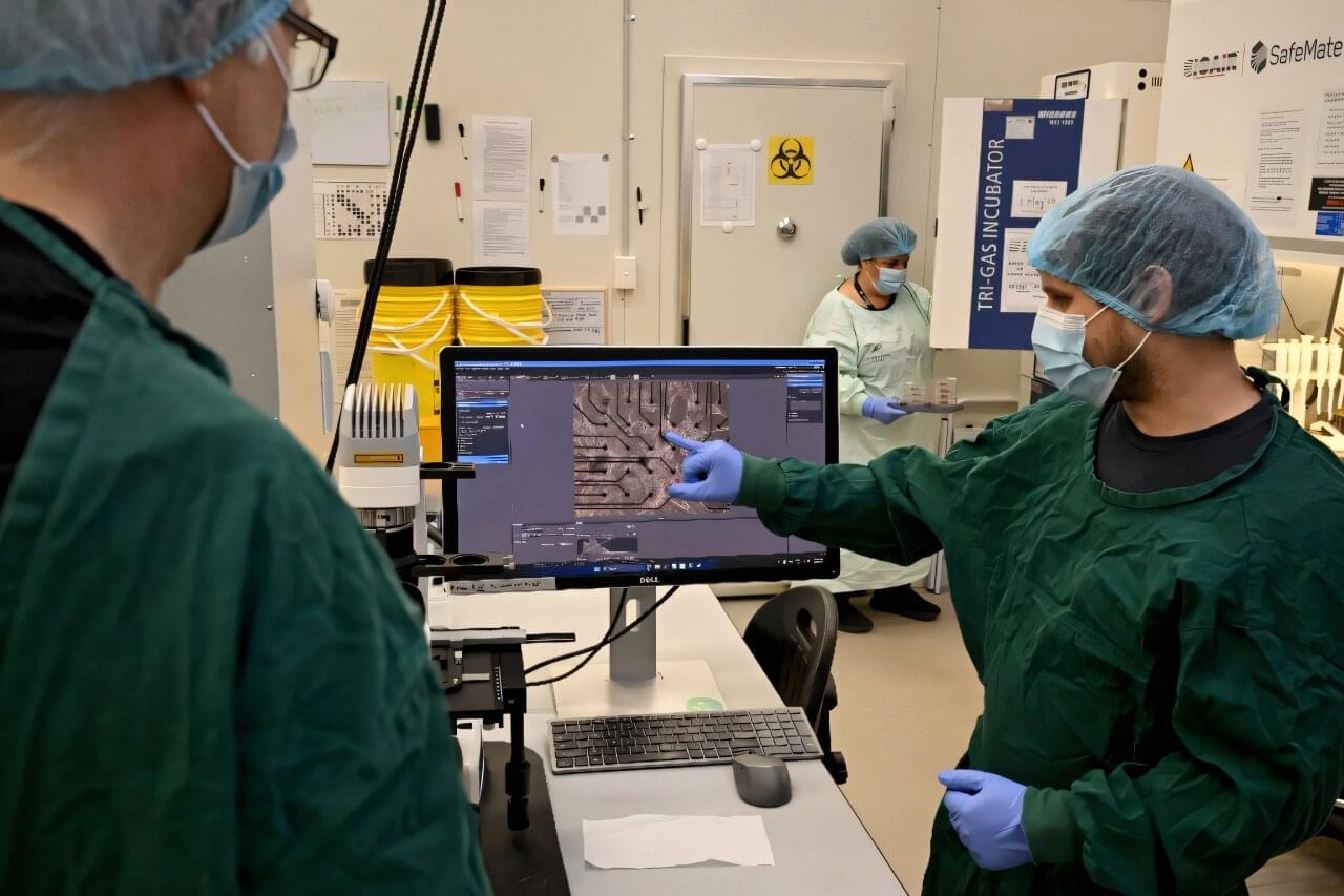
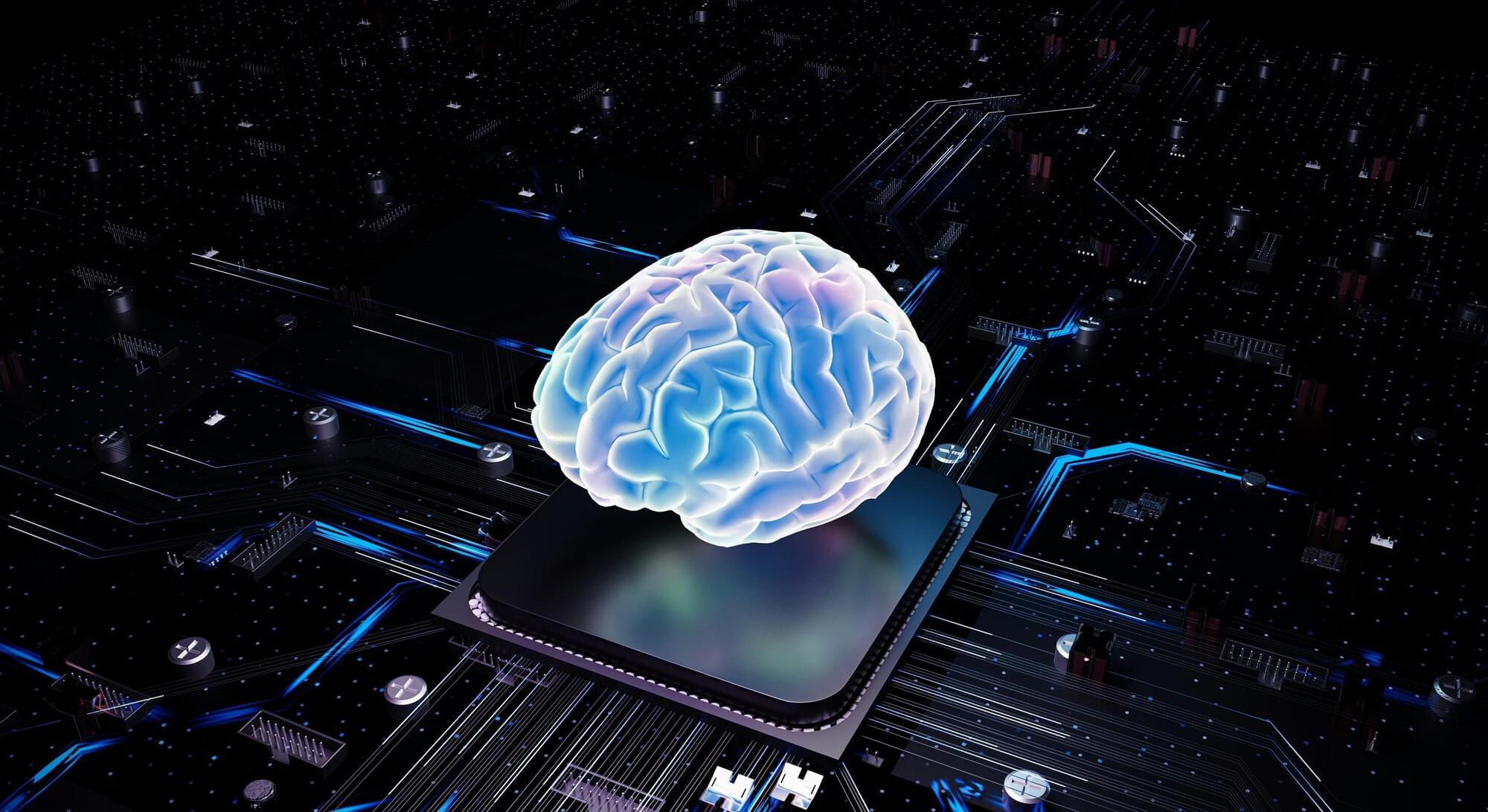
Australian researchers have trained lab-grown brain cells on a silicon computer chip to play the nineties shooter game “Doom” and say they are just scratching the surface of what the neurons could be capable of doing.
It’s the science-fiction work of biotech boffins at Cortical Labs, who researched and developed the technology that harnesses the workings of the brain’s networking system.
Each so-called “biological computer” contains around 200,000 living human brain cells, grown from stem cells that were harvested from blood donations.
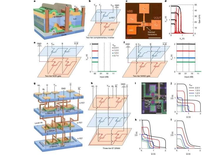
Through new research published in Nature, Qing Cao and colleagues at the University of Illinois Urbana-Champaign have developed a new approach that sidesteps these problems, bringing high-performance 3D chips a step closer to reality.
Overheated stacks of transistors
Modern computer chips are built on thin wafers of silicon, with transistors (the tiny switches that process information) arranged in a single flat layer. If multiple layers of transistors could instead be stacked on top of each other on the same chip, it would dramatically increase their density without enlarging the chip’s footprint. However, this 3D design would cause the chip to overheat, which could destroy the circuitry already laid down beneath it.
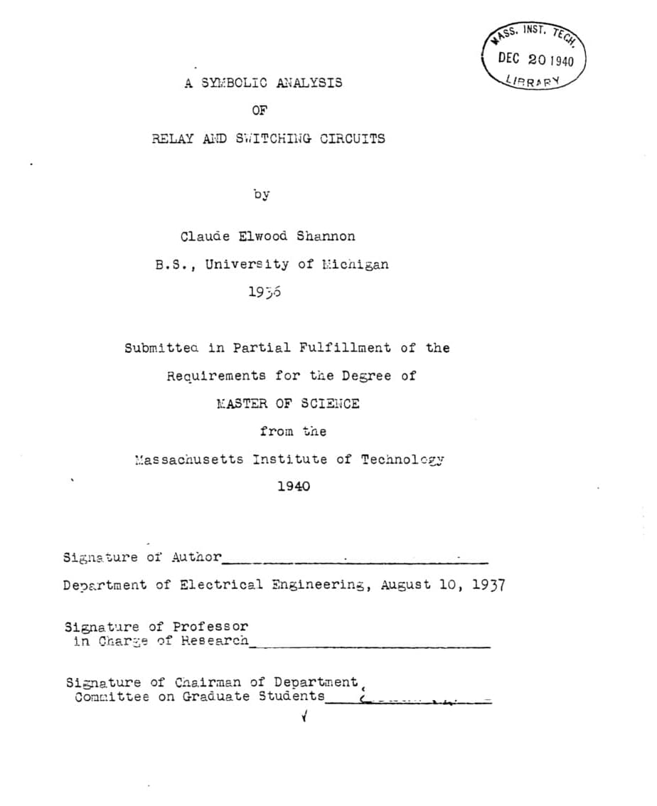
In 1937, a young graduate student named Claude Shannon submitted a master’s thesis with an unassuming title: “A Symbolic Analysis of Relay and Switching Circuits.”
A Symbolic Analysis of Relay and Switching Circuits is the title of a master’s thesis written by computer science pioneer Claude E. Shannon while attending the Massachusetts Institute of Technology (MIT) in 1937, [ 1 ] [ 2 ] and then published in 1938. In his thesis, Shannon, a dual degree graduate of the University of Michigan, proved that Boolean algebra [ 3 ] could be used to simplify the arrangement of the relays that were the building blocks of the electromechanical automatic telephone exchanges of the day. He went on to prove that it should also be possible to use arrangements of relays to solve Boolean algebra problems. His thesis laid the foundations for all digital computing and digital circuits. [ 4 ] [ 5 ]
The utilization of the binary properties of electrical switches to perform logic functions is the basic concept that underlies all electronic digital computer designs. Shannon’s thesis became the foundation of practical digital circuit design when it became widely known among the electrical engineering community during and after World War II. At the time, the methods employed to design logic circuits (for example, contemporary Konrad Zuse’s Z1) were ad hoc in nature and lacked the theoretical discipline that Shannon’s paper supplied to later projects.
Shannon’s work also differed significantly in its approach and theoretical framework compared to the work of Akira Nakashima. Whereas Shannon’s approach and framework was abstract and based on mathematics, Nakashima tried to extend the existent circuit theory of the time to deal with relay circuits, and was reluctant to accept the mathematical and abstract model, favoring a grounded approach. [ 6 ] Shannon’s ideas broke new ground, with his abstract and modern approach dominating modern-day electrical engineering. [ 6 ].
A feature story authored by Simon Spichak, MSc investigates how biotech companies like Cortical Labs and FinalSpark harness human brain cells to electrodes, performing computational functions and testing the cells’ responses to electrical and chemical stimuli. To create biocomputers, scientists grow organoids—small spheres of, in this case, neural tissue—on top of multi-electrode arrays in a hardware shell, which can then be used for everything from testing medications to playing video games. The work is published in the Journal of Medical Internet Research.
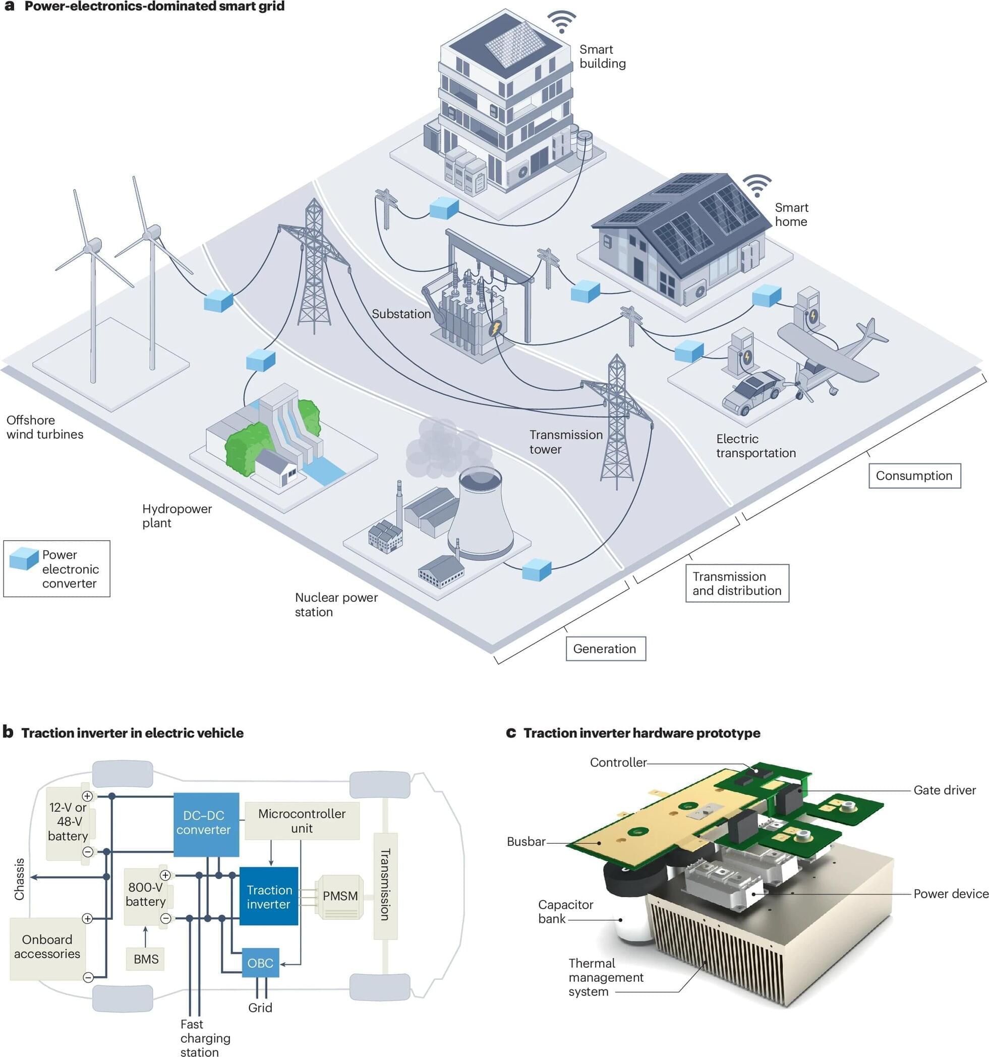
Modern power systems are rapidly evolving into highly digitized smart grids, increasing their complexity at an unprecedented pace. Renewables, batteries, electric vehicles, power electronics, sensors and real-time control systems are all expanding rapidly, and this is making electricity grids significantly harder to simulate, optimize, secure and operate.
This is driven by the increasing energy demands of a tech-driven modern world. Think of a suburban street in 2005—every house pulled electricity from the grid, and power flowed in one direction from big power stations.
This same street in 2026 might have houses with rooftop solar exporting power back into the grid; electric vehicles (EVs) that need to charge overnight; home batteries storing solar energy and feeding it back into the grid when prices spike; electric busses, electric irrigation pumps, automated machinery and smart appliances that turn on and off based on grid signals.

Google says the Chrome Device Bound Session Credentials (DBSC) security feature is now generally available and is rolling out to all users to prevent account takeovers.
Available in beta since April, DBSC was first announced in 2024 as a way to cryptographically bind session cookies to a specific device, preventing hackers from using such stolen cookies to bypass multi-factor authentication (MFA) and hijack users’ accounts.
DBSC works by cryptographically linking user sessions to the hardware, such as their computer’s security chip (e.g., the Trusted Platform Module (TPM) on Windows and the Secure Enclave on macOS).