“The Self as Software: Transcending and Enhancing the Brain” presented by Susan Schneider. Co-sponsored by Cognitive Science, Computing Sciences, and Philosophy
Category: computing – Page 12
Meta wants to replace your mouse and keyboard with this bracelet
face_with_colon_three year 2025.
Researchers at Meta have developed a wristband that translates your hand gestures into commands to interact with a computer, including moving a cursor, and even transcribing your handwriting in the air into text. It could make today’s personal devices a lot more accessible to people with reduced mobility or muscle weakness, and even unlock new ways for people to control their gadgets effortlessly.
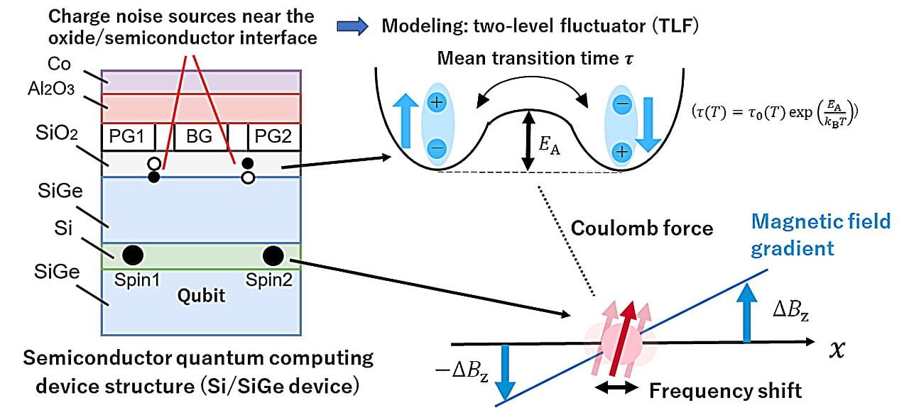
Scientists identify the origin of noise in spin qubit quantum processors
A spin qubit, in which quantum information is encoded in the spin state of an electron, is one of the most promising platforms for quantum computing. Spin qubits exhibit long coherence times and are compatible with advanced semiconductor manufacturing technologies. The leading implementation of spin qubits involves confined electrons inside quantum dots, a nanoscale semiconductor architecture that behaves like a controllable artificial atom. Recent advances have enabled high-fidelity operation of single- and two-qubit gates, exceeding the threshold required for certain surface code quantum error correction techniques.
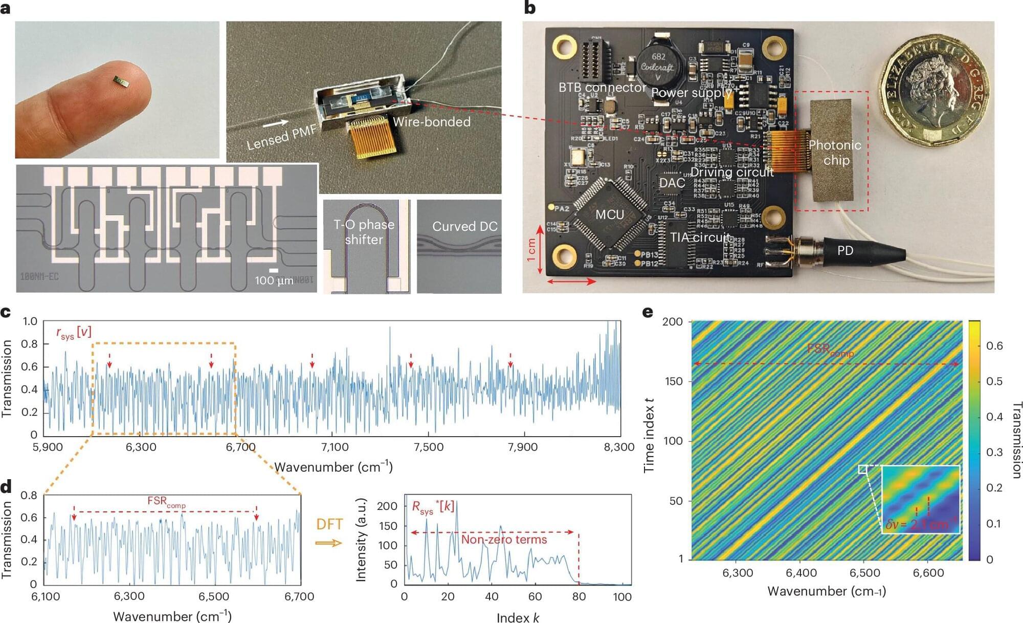
Why this $10 spectrometer chip could bring real-time chemical sensing to wearables
Researchers from the University of Cambridge and GlitterinTech, a startup founded by the same research group, have unveiled a fundamentally new type of optical spectrometer that delivers laboratory-grade precision in a device small enough to be embedded in portable and wearable technologies. By rethinking how spectra are measured and processed, the team has demonstrated a spectrometer costing only around $10, operating at a centimeter scale, and capable of applications ranging from industrial quality control to real-time health care monitoring.
Optical spectrometers underpin countless technologies, from chemical analysis and manufacturing to environmental sensing and medicine. Yet shrinking these instruments has historically involved painful trade-offs: Miniaturized devices typically sacrifice bandwidth, resolution or accuracy, limiting them to rough identification rather than true metrological measurements. The newly reported convolutional spectrometer overcomes these barriers by introducing a conceptually elegant operating principle grounded in the convolution theorem, offering unprecedented performance metrics compared with existing dispersive, Fourier-transform and reconstructive spectrometers.
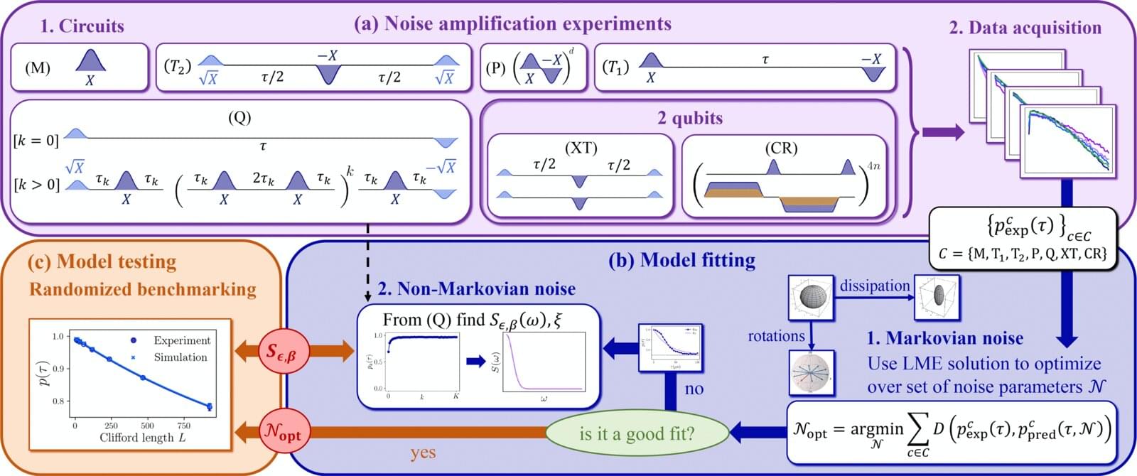
Cloud-tested quantum noise model predicts superconducting qubit errors with sevenfold better accuracy
Researchers from the Johns Hopkins Applied Physics Laboratory (APL) in Laurel, Maryland, and Johns Hopkins University in Baltimore have developed a practical, comprehensive noise-modeling framework for a popular class of superconducting quantum processors. Their work, published in the journal PRX Quantum, offers a sevenfold improvement in predictive accuracy over existing approaches.
Quantum bits, or qubits, are intrinsically prone to noise—interference arising from environmental factors such as electrical and magnetic fields or temperature fluctuations—as a result of the extreme sensitivity that makes them so valuable for computing. Developing accurate noise models is key to creating the robust quantum algorithms and resilient error-correction protocols required to build truly fault-tolerant quantum computers.
“To really advance the field, we need models that can predict a wide range of behavior while utilizing a small number of parameters, rather than theoretical models that try to account for all of the fundamental physics at play in quantum interactions,” said project lead Gregory Quiroz, a senior physicist at APL and an associate research professor in the Department of Physics and Astronomy at the Johns Hopkins University Krieger School of Arts and Sciences. “The novelty of our approach lies in a unified and experimentally validated framework that connects multiple noise mechanisms and yields a coherent predictive methodology.”
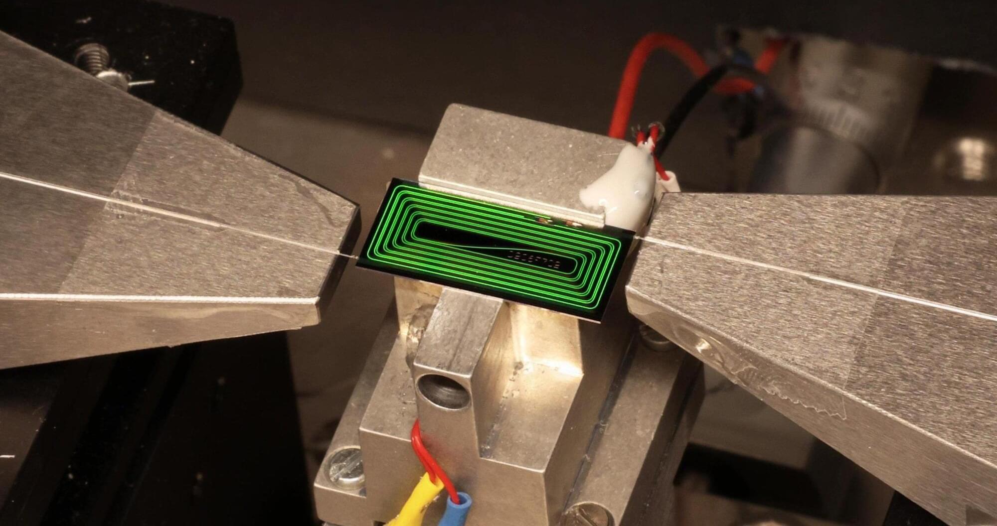
New cryogenic silicon carbide hardware addresses quantum computing bottleneck
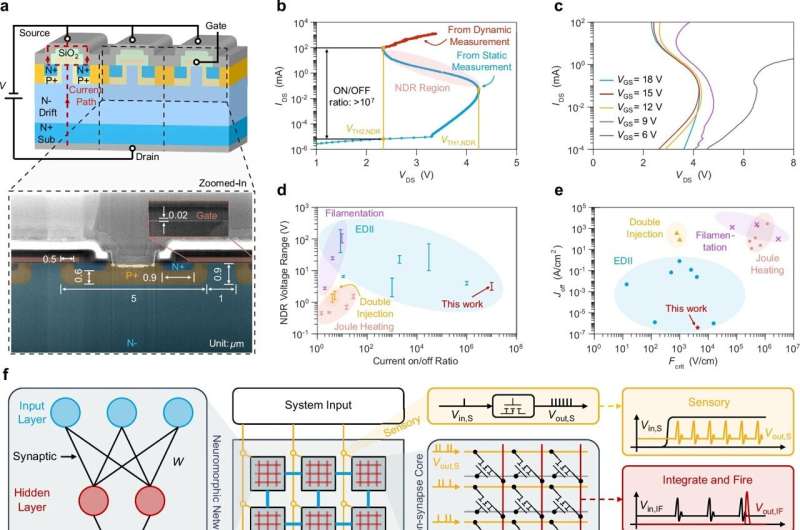
Researchers from the Department of Electrical and Computer Engineering in the Faculty of Engineering at the University of Hong Kong (HKU) and the Centre for Advanced Semiconductors and Integrated Circuits (CASIC) have achieved a major breakthrough in cryogenic electronics. The team has developed a programmable neuromorphic hardware platform that operates near absolute zero, providing a potential solution for scaling up quantum computers and enabling deep-space exploration. The discovery was published in Nature Communications in an article titled “Cryogenic neuromorphic circuits using gate-controlled negative differential resistance in silicon carbide.”
Led by Professor Yuhao Zhang and Ph.D. student Xin Yang, the team discovered an innovative way to generate and control negative differential resistance (NDR) in industry-standard silicon carbide (SiC) MOSFETs. For the first time, they demonstrated that a single transistor can mimic the energy-efficient “spiking” behavior of biological neurons at temperatures as low as 10 mK.
Modern quantum computers rely on complex electronics to control qubits, which are extremely sensitive and must be maintained at millikelvin temperatures. Current silicon-based controllers generate excessive heat and consume high levels of power, forcing them to be placed far from the qubits. This separation creates a wiring bottleneck that limits the scalability and performance of quantum systems.
Physicists create new family of Schrödinger-cat states
Quantum mechanics, unlike classical physics, allows objects to exist in more than one state at the same time. This idea is often illustrated by Schrödinger’s cat, imagined as being both alive and dead until it is observed. In the laboratory, physicists can create less dramatic but very real versions of this effect by placing atoms, light or motion into two distinct quantum states at once. Creating and controlling these superpositions is essential for applications ranging from quantum computing to precision timekeeping.
A simple example is a quantum bit, or qubit, in a superposition of both 0 and 1. But quantum systems are not limited to just two states. In a quantum harmonic oscillator, which can occupy many different energy levels, there is a much richer set of possibilities. Quantum harmonic oscillators describe many physical systems, including light, vibrations and the motion of trapped particles, and have been used to create a wide variety of quantum superpositions. One well-known example is a “cat state,” in which an oscillator is placed in a superposition of two wave packets displaced in opposite directions. These wave packets, known as coherent states, resemble classical motion as closely as quantum mechanics allows.
Researchers at the University of Oxford have now demonstrated a new family of quantum superpositions. Instead of building catlike states from coherent-state wave packets, they developed a method for creating superpositions from a broad range of components that are themselves highly nonclassical. In examples such as squeezed-state superpositions, quantum uncertainty is redistributed differently in each part of the state. The research is published in the journal Physical Review X.
Nickelate superconductors share a common electronic fingerprint
Superconductors, materials that conduct electricity with zero electrical resistance at specific temperature ranges, have proved very promising for the development of quantum computers and other cutting-edge technologies. While most of these materials become superconducting at very low temperatures, others exhibit superconductivity at higher temperatures.
Two types of materials that are known to be high-temperature semiconductors are cuprates (i.e., compounds containing negatively charged copper ions) and nickelates (i.e., compounds that contain negatively charged nickel-oxygen ions). While cuprates have been known to be superconductors for decades, nickelates were only recently found to exhibit superconductivity at unusually high temperatures.
Researchers at University of British Columbia (UBC), Argonne National Laboratory, and the Canadian Light Source (CLS), carried out a study aimed at better understanding how the electronic structure of nickelates contributes to their superconductivity.
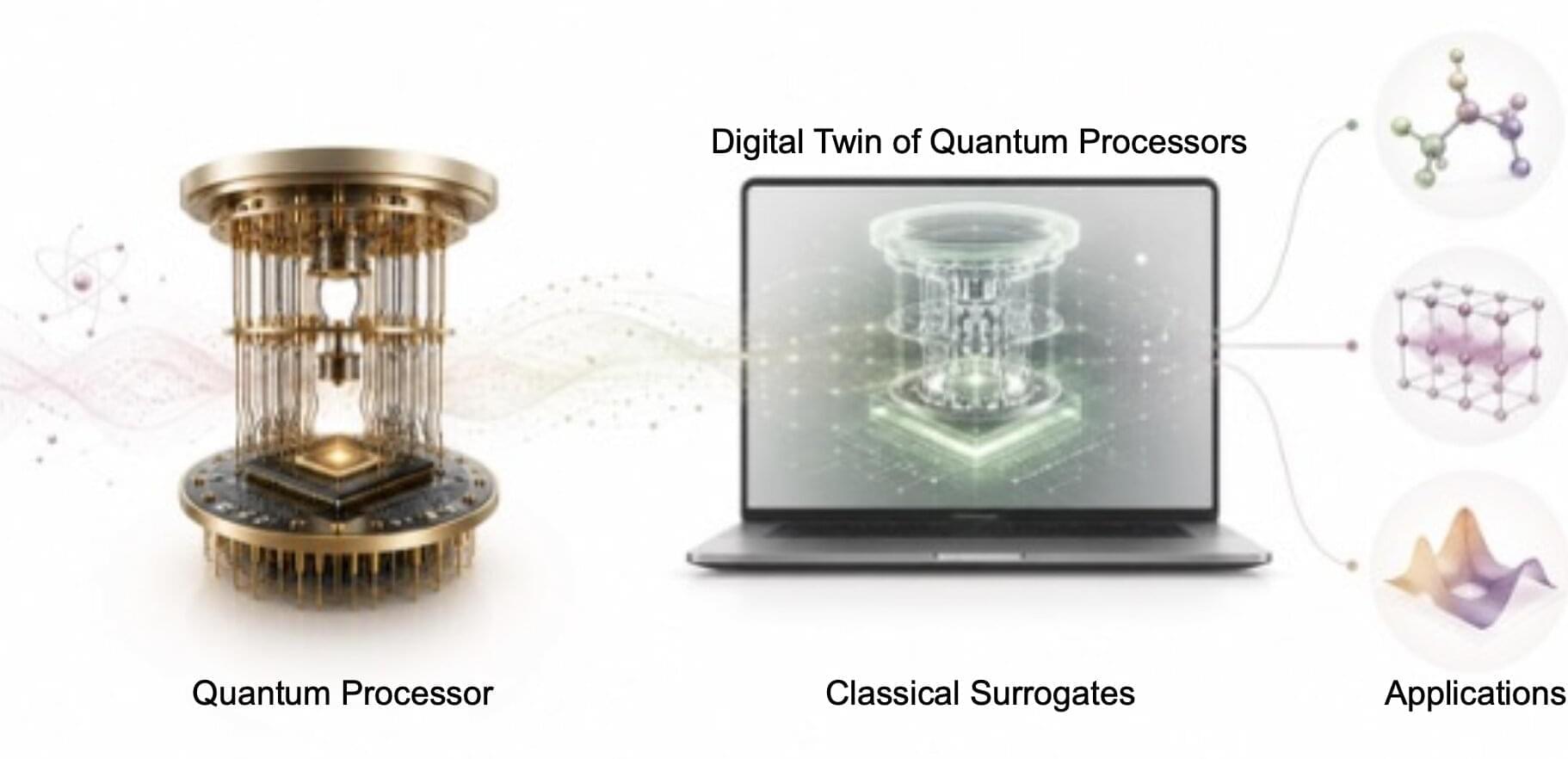
Predictive surrogates could cut quantum computing measurement overhead by more than 99.97%
Quantum computers, systems that process information leveraging quantum mechanical effects, have the potential of outperforming classical computers on some tasks. Despite their potential, the use of these systems remains very limited, due to their high cost and other challenges that have so far prevented their large-scale fabrication.
Researchers at the Henan Key Laboratory of Quantum Information and Cryptography and Nanyang Technological University have developed predictive surrogates, new computational models that can learn and reproduce the outputs of quantum processors.
These models, introduced in a paper published in Nature Communications, could be used to extract useful information from quantum computers and perform computations more efficiently with provable guarantees, even if users do not have direct access to advanced and expensive quantum computing hardware.