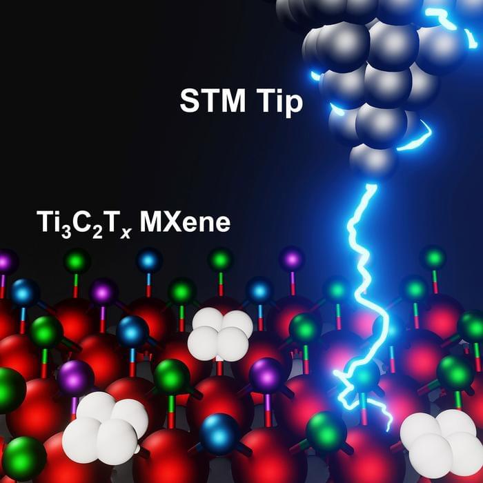
In the decade since their discovery at Drexel University, the family of two-dimensional materials called MXenes has shown a great deal of promise for applications ranging from water desalination and energy storage to electromagnetic shielding and telecommunications, among others. While researchers have long speculated about the genesis of their versatility, a recent study led by Drexel and the University of California, Los Angeles, has provided the first clear look at the surface chemical structure foundational to MXenes’ capabilities.
Using advanced imaging techniques, known as scanning tunneling microscopy (STM) and scanning tunneling spectroscopy (STS), the team, which also includes researchers from California State University Northridge, and Lawrence Berkeley National Laboratory, mapped the electrochemical surface topography of the titanium carbide MXene — the most-studied and widely used member of the family.
Their findings, published in the 5th anniversary issue of the Cell Press journal Matter (“Atomic-scale investigations of Ti 3 C 2 Tx MXene surfaces”), will help to explain the range of properties exhibited by members of the MXene family and allow researchers to tailor new materials for specific applications.
