Researchers at Kyushu University, the National Institute of Advanced Industrial Science and Technology (AIST) and Osaka University in Japan have recently introduced a new strategy for synthesizing multi-layer hexagonal boron nitride (hBN), a material that could be used to integrate different 2D materials in electronic devices, while preserving their unique properties. Their proposed approach, outlined in a paper published in Nature Electronics, could facilitate the fabrication of new highly performing graphene-based devices.
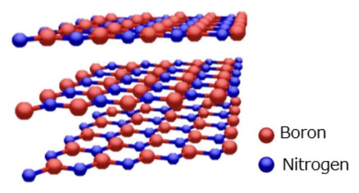
“The atomically flat 2D insulator hBN is a key material for the integration of 2D materials into electronic devices,” Hiroki Ago, one of the researchers who carried out the study, told Tech Xplore. “For example, the highest carrier mobility in monolayer graphene is achieved only when it is sandwiched by multilayer hBN. Superconductivity observed in twisted bilayer graphene also needs multilayer hBN to isolate from environment.”
In addition to its value for fabricating graphene-based devices, hBN can also be used to integrate transition metal dichalcogenides (TMDs) in devices, achieving strong photoluminescence and high carrier mobility. It can also be valuable for conducting studies focusing on moiré physics.