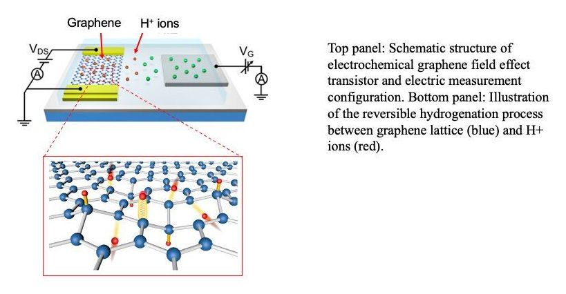
Over the past decade or so, the semimetal graphene has attracted substantial interest among electronics engineers due to its many advantageous qualities and characteristics. In fact, its high electron mobility, flexibility and stability make it particularly desirable for the development of next-generation electronics.
Despite its advantageous properties, large-area graphene has a zero bandgap (i.e., the energy range in solid materials at which no electronic states can exist). This means that electric current in graphene cannot be completely shut off. This characteristic makes it unsuitable for the development of many electronic devices.
Researchers at Tsinghua University in China recently devised a design strategy that could be used to attain a larger bandgap in graphene. This strategy, introduced in a paper published in Nature Electronics, entails the use of an electric field to control conductor-to-insulator transitions in microscale graphene.
