Truthfully, it has been some time since Moore’s law, the propensity for processors to double in transistor count every two years, has been entirely accurate. The fundamental properties of silicon are beginning to limit development and will significantly curtail future performance gains, yet with 50 years and billions invested, it seems preposterous that any ‘beyond-silicon’ technology could power the computers of tomorrow. And yet, Nano might do just that, by harnessing its ability to be designed and built like a regular silicon wafer, while using carbon to net theoretical triple performance at one-third the power.
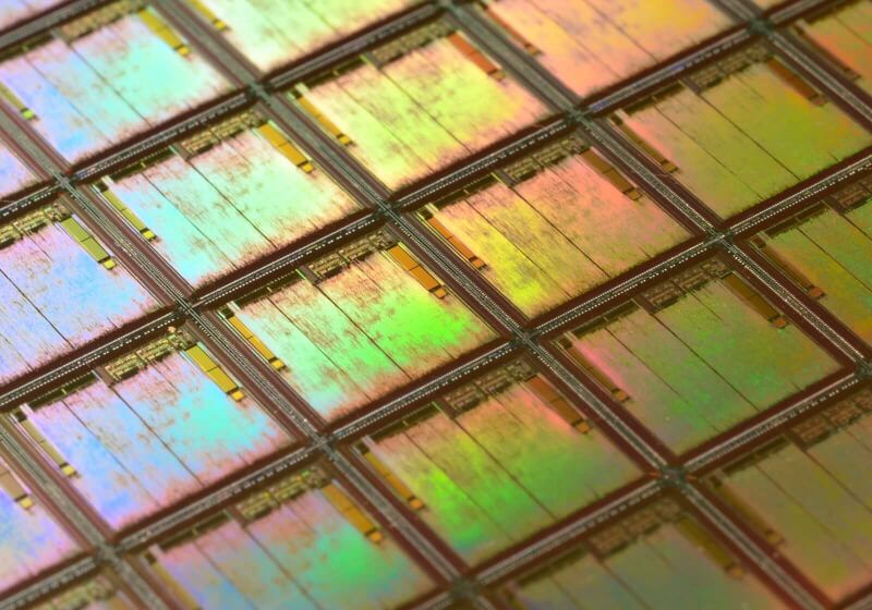
Nano began life much like all processors, a 150mm wafer with a pattern carved out of it by a regular chip fab. Dipped into a solution of carbon nanotubes bound together like microscopic spaghetti, it re-emerged with its semi-conductive carbon nanotubes stuck in the pattern of transistors and logic gates already etched on it. It then undergoes a process called ‘RINSE,’ removal of incubated nanotubes through selective exfoliation, by being coated with a polymer then dipped in a solvent. This has the effect of reducing the CNT layer to being just one tube, removing the large clumps of CNTs that stick together over 250 times more effectively than previous methods.
One of the challenges facing CNT processors has been difficulty in separating N-type and P-type transistors, which are “on” for 1 bit and “off” for 0 bit and the reverse, respectively. The difference is important for binary computing, and to perfect it, the researchers introduced ‘MIXED,’ metal interface engineering crossed with electrostatic doping. Occurring after RINSE, small platinum or titanium components are added to each transistor, then the wafer is coated in an oxide which acts as a sealant, improving performance. After that, Nano was just about done.
