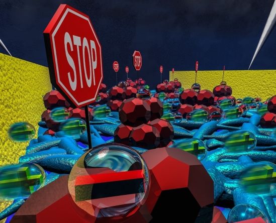
In what could be called a classic “Eureka” moment, UC Santa Barbara materials researchers have discovered a simple yet effective method for mastering the electrical properties of polymer semiconductors. The elegant technique allows for the efficient design and manufacture of organic circuitry (the type found in flexible displays and solar cells, for instance) of varying complexity while using the same semiconductor material throughout.
“It’s a different strategy by which you can take a material and change its properties,” said Guillermo Bazan, a professor of chemistry and materials at UCSB. With the addition of fullerene or copper tetrabenzoporphyrin (CuBP) molecules in strategic places, the charge carriers in semiconducting materials—negative electrons and positive “holes”—may be controlled and inverted for better device performance as well as economical manufacture. The discovery is published in a pair of papers that appear in the journals Advanced Functional Materials and Advanced Electronic Materials.
In the realm of polymer semiconductors, device functionality depends on the movement of the appropriate charge carriers across the material. There have been many advances in the synthesis of high-mobility, high-performance materials, said lead author Michael Ford, graduate student in materials, but the fine control of the electrons and holes is what will allow these sophisticated polymers to reach their full potential.
